
Optical Diagnostics for Thin Film Processing
Irving P. Herman
- 783 pages
- English
- ePUB (adapté aux mobiles)
- Disponible sur iOS et Android
Optical Diagnostics for Thin Film Processing
Irving P. Herman
À propos de ce livre
This volume describes the increasing role of in situ optical diagnostics in thin film processing for applications ranging from fundamental science studies to process development to control during manufacturing. The key advantage of optical diagnostics in these applications is that they are usually noninvasive and nonintrusive. Optical probes of the surface, film, wafer, and gas above the wafer are described for many processes, including plasma etching, MBE, MOCVD, and rapid thermal processing. For each optical technique, the underlying principles are presented, modes of experimental implementation are described, and applications of the diagnostic in thin film processing are analyzed, with examples drawn from microelectronics and optoelectronics. Special attention is paid to real-time probing of the surface, to the noninvasive measurement of temperature, and to the use of optical probes for process control.
Optical Diagnostics for Thin Film Processing is unique. No other volume explores the real-time application of optical techniques in all modes of thin film processing. The text can be used by students and those new to the topic as an introduction and review of the subject. It also serves as a comprehensive resource for engineers, technicians, researchers, and scientists already working in the field.
- The only volume that comprehensively explores in situ, real-time, optical probes for all types of thin film processing
- Useful as an introduction to the subject or as a resource handbook
- Covers a wide range of thin film processes including plasma etching, MBE, MOCVD, and rapid thermal processing
- Examples emphasize applications in microelectronics and optoelectronics
- Introductory chapter serves as a guide to all optical diagnostics and their applications
- Each chapter presents the underlying principles, experimental implementation, and applications for a specific optical diagnostic
Foire aux questions
Informations
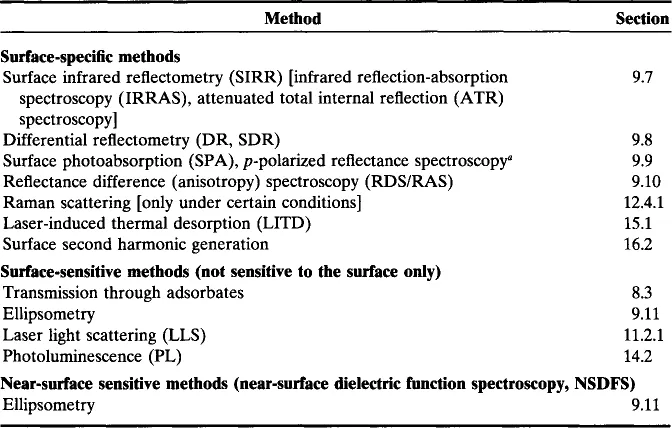
Overview of Optical Diagnostics
| Metal CVD | Wafer temperature (real-time) |
| Sheet resistance (endpoint) | |
| Metal film thickness, surface roughness (post-processing) | |
| Dielectric CVD | Wafer temperature (real-time) |
| Film thickness (endpoint) | |
| Particles (in gas, on wafer; real-time, post-processing) | |
| Refractive index, film stress (post-processing) | |
| Silicon CVD/epitaxy | Wafer temperature (real-time) |
| Film thickness (endpoint) | |
| Particles (in gas, on wafer; real-time, post-processing) | |
| Grain size (post-processing) [polycrystalline] | |
| Sheet resistance, surface reflectance (post-processing) | |
| Plasma etch (anisotropic/isotropic, ashing) | Plasma power, plasma density (real-time) |
| Particles (in gas, on wafer; real-time, post-processing) | |
| Film thickness, plasma emission (endpoint) | |
| Critical dimension (real-time, post-processing) [anisotropic etch] | |
| Anisotropy, side-wall angle, overetch (real-time, post-processing) | |
| Selectivity (post-processing) | |
| Thermal oxidation/nitridation | Wafer temperature (real-time) |
| Film thickness, slips, thickness uniformity (post-processing) | |
| Implant activation and drive-in | Wafer temperature, dopant dose and energy (real-time) |
| Electrical activation (endpoint) | |
| Sheet resistance, slips (post-processing) | |
| Resist processing | Resist thickness, uniformity (post-coating, pre-exposure) |
| Latent image, image overlay (during exposure) | |
| Surface condition, plasma emission (dry-develop endpoint) | |
| Critical dimension (post-processing) | |
| Glass reflow | Wafer temperature (real-time) |
| Surface topography (endpoint) | |
| Film thickness, stress (pre- and post-processing) |
| Method | Measuring | Monitoring |
| Optical | ||
| Optical emission spectroscopyab (Section 6.3.1.2) | Spectrum of light emitted from discharge and its intensity | Emission from reactive species and/or etch products |
| Absorptionb(Chapter 8; Section 8.3 for films) | Transmitted light | Change in concentrations in different molecules. |
| Optical reflection (Sections 9.4, 9.5, 9.11) | Reflection changes, interference effects,bc or ellipsometry parameter monitoring | Changes in film thickness |
| Scatterometryb (Section 11.2) | Diffracted light | The profile of the surface or of the refractive index distribution. |
| Pyrometry (thermal imaging) (Section 13.2) | Infrared emission | Changes in emissivity |
| Photoemission optogalvanic spectroscopya (Section 17.3) | Plasma current | Changes in work function due to changed surface |
| Nonoptical | ||
| Mass spectrometry | Gas composition | Etch products |
| Impedance monitoringa | Impedance mismatch | Voltage change |
| Langmuir probea | Changes in electron density or average energy | Current from probe |
| Pressure | Total pressure | Changes in total pressure |
| Method | Section |
| OESa | 6.3 |
| LIF | 7.2 |
| Infrared diode laser absorption spectroscopy (IR-DLAS) | 8.2.1.1 |
| Fourier transform infrared spectroscopy (FTIRS) | 8.2.1.2 |
| Ultraviolet/visible absorption | 8.2.2 |
| Interference holography | 10.1 |
| Raman scattering | 12.3 |
| CARS | 16.1 |
| Third harmonic generation (THG) | 16.3 |
| REMPI | 17.1 |