Intended title: A Hybrid BJT/FET Power Amplifier
This was the first article on power amplifiers that I published, though I had been designing them for manufacture since 1975. This investigation into the concept of combining power FET output devices with bipolar drivers was done some years before I undertook my major investigation into the root causes of power amplifier distortion (see ‘Distortion in Power Amplifiers’, Parts 1–8, later in this book), which led in turn to the book Audio Power Amplifier Design [1]. In the throes of the design process, I realised with greater force than hitherto that the distortions in the small-signal part of a power amplifier were (a) far from negligible and (b) susceptible to analysis by a mixture of SPICE simulation and a few well-chosen experiments. I also determined that SPICE could be extremely useful in the analysis of output stages, if used to create an incremental gain plot.
Delving back into my history of power amplifier design, I note that at this stage I wasn’t all that enthusiastic about DC-coupled power amplifiers. The ‘kamikaze krowbars’ mentioned were the sort of untrustworthy and unworkable compromise that was sometimes adopted before everyone realised that a DC-coupled amplifier really did have to be fitted with proper offset-detection and a reliable relay capable of breaking the fault current. The crowbar was a triac (so it could conduct both ways) connected across the amplifier output, and triggered via a simple RC lowpass filter. It usually only triggered once because to protect the loudspeaker, the entire charge of the reservoir capacitors had to be shorted to ground, exploding the triac and vaporising its associated PCB tracking. If it triggered when it should not, it would probably destroy perfectly sound output devices as well, by putting a dead short across the output that would severely test the short-circuit protection. Essentially it was a matter of destroying the amplifier to save the speaker, much as an expensive power transistor will sacrifice itself to save a fuse. It was a rotten idea but it was perpetrated by at least one much respected company that should have known better. Compared with this sort of thing, an output capacitor seemed delightfully simple, though in those days I did not know much about the higher distortion that can occur when you put large signal currents through electrolytic capacitors [2]. Putting the output capacitor at least partly inside the global negative feedback loop should help, but it’s not so easy to do.
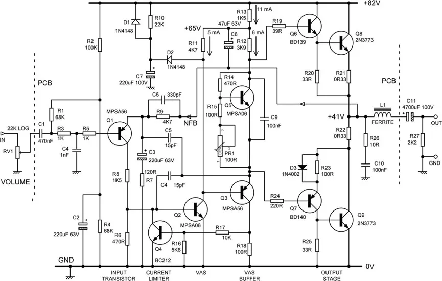
It might be of interest to give some details of the last AC-coupled power amplifier I designed, and if not you’re going to get them anyway. It was a 100W/8Ω design developed around 1979 for multiple applications, including driving big intercom rings in large venues. Reliability and low cost rather than high-end hi-fi was the prime directive, and so it had a quasi-complementary output stage using two 2N3773s in TO-3 packages. These parts had a reputation for being tough high-voltage devices, and were used in the famous Crown DC300 amplifiers. They were supplied to us by Jermyn. Nowadays the 2N3773 is showing its age, with an unimpressive minimum beta of 15 at an Ic of8 Amps, falling to a feeble 5 at the maximum Ic of 16 Amps according to the manufacturer’s data sheet. The output coupling capacitor was 4700uF/100V, which was twice the size normally used, and in those days a pretty hefty component. The schematic is shown in Preface Figure 20.1.
There is a single input transistor Q1 which performs the feedback subtraction; in an AC-coupled amplifier the DC precision of a differential input pair is not necessary. The second-harmonic generated by a single transistor was acceptable for this application and the parts count was minimised. Q1 is a transconductance stage in the same way as a differential pair, and it passes its output current into the base of VAS Q2. A VAS buffer Q3 prevents the output stage loading the VAS and is included in the loop of dominant-pole capacitor C4. This arrangement was inspired by the Equin amplifier published in one of the first issues of Elektor in 1976 [3], though no other Equin features were adopted apart from the use of capacitor output coupling. I have no recollection as to why C5 was included; it looks like a nod to the ‘input-inclusive compensation’ often advocated by John Linsley-Hood. All I can say at this point is that the amplifier was reliably stable. The collector of the VAS and the emitter of the VAS buffer are bootstrapped by C8, my thinking being that it would be preferable to using two current sources because it would be more reliable, with no transistors to fail, and more economical because resistors were then significantly cheaper than transistors; also there was no need for biasing components for current-sources. Q4 acts as a current-limiter for the VAS buffer Q3, to prevent it passing excessive current when in negative clipping or SOAR protection, as it attempts to obey the negative feedback and pull the output down; looking back at the old schematics, I was surprised that I was using this technique so early. It is usually very necessary if an amplifier is survive prolonged clipping, but does not appear in all designs by any means. Standard single-slope SOAR limiting was fitted; this is not shown in the schematic for clarity.
The output stage is a standard quasi-complementary configuration with a Baxandall diode (D3). Looking back, I wonder if the value of R23 should have been adjusted to match that of R25. The output emitter resistors R21 and R22 are 0.33 Ω; nowadays I would make them 0.1 Ω, which would give better linearity at the cost of increased quiescent current.
The output inductor L1 followed contemporary practice, being a very small component as it was a VHF suppression choke wound on a small ferrite core; what this core might have done to the linearity I do not know. I thought up a beautifully simple RC network for de-thumping at switch-on and no output relay was required. When amplifiers with this sort of input stage are switched on, they usually make an almighty bang. This is despite the large value of filter capacitor C2, which makes the bias voltage come up slowly. The problem is that as the bias comes up, Q1 remains firmly off because of the extra delay in charging C3 via feedback resistor R9. As a result the VAS collector, and therefore the amplifier output, shoots up at the same rate as the supply rail rises, rather than rising slowly with the voltage on C2. This is effectively prevented by adding C7, R10, and D2; the VAS collector can now only rise slowly because it has to charge C7 with a limited amount of current. C7 is also charged by R10, and eventually reaches rail voltage, and D2 is reverse-biased even at full output swing. With the means of measurement available to me, the presence of a reverse-biased D2 seemed to have no ill-effects on linearity. D1 is intended to speed-up the discharge of C7 on powering down.
The single supply rail reduced PSU costs somewhat compared with dual-rail; there was a single 4700uF/100V reservoir capacitor for two channels. The output capacitor C11 makes short-circuit protection easier because however low the load impedance, only one capacitor’s worth of electrical charge can be transferred per cycle. I don’t recall ever hearing that one of these amplifiers had failed.
The construction was, naturally, somewhat old-school. The amplifier PCBs were single-sided, with no solder-resist (the company concerned soldered everything manually—no wave-soldering then) and no component ident, once again to keep costs down. That may sound silly but with the technology of the day, adding a silk-screen component ident added significant cost; it also had to be tediously laid out by hand on plastic film with Letraset rather than generated automatically by a CAD package. I succeeded in laying out the PCB without a single link being necessary; back in the day this saved assembly time and got definite kudos. As usual this required some rather convoluted routing of noncritical tracks. Now that PTH PCBS are so economical, this sort of thing is probably becoming a lost art.
Preface Figure 20.1 My quasi-complementary 100W/8Ω power amplifier, circa 1979: protection circuitry omitted for clarity
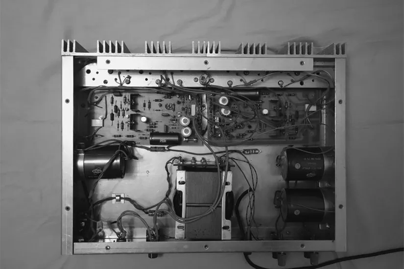
Preface Figure 20.2 Two 100W/8Ω quasi-complementary power amplifier modules make up a stereo amplifier, circa 1979.
A stereo amplifier using two of the amplifier PCBs is shown in Preface Figure 20.2 The output transistors are mounted on the underside of the extrusion at the top; in its cent...