- 208 pages
- English
- ePUB (mobile friendly)
- Available on iOS & Android
eBook - ePub
About this book
Nucleation and Growth of Metals: From Thin Films to Nanoparticles explores how nucleation and growth phenomena condition the morphology and related characteristics of metallic thin films and nanoparticles to help control the functional properties of these objects.
The book brings a rigorous theoretical approach to nucleation and growth phenomena, with a particular focus on the essential aspects and outcomes of this theory. The author explores a general framework for the nucleation and growth of condensed phases from liquid solutions. Practical situations are extensively described, providing state-of-the art information on Cu electroplating and related processes for the fabrication of advanced interconnects and elaboration of metallic nanoparticles.
- Derives the basic equations of nucleation from fundamental thermodynamic and kinetic relations
- Explores the main outcomes of a range of nucleation theories
- Features practical examples to further develop the theoretical aspects
- Provides state-of-the art information on Cu electroplating and related processes for the fabrication of advanced interconnects and elaboration of metallic nanoparticles
Trusted by 375,005 students
Access to over 1.5 million titles for a fair monthly price.
Study more efficiently using our study tools.
Information
1
The Fabrication of Micro- and Nanostructures
Abstract
As Feynman first stated in his visionary lecture in 1959, there is plenty of room at the bottom. Indeed, the source of most of our current technological progresses is our ability to manipulate and shape matter at a very small size, down to the nanometer scale. In this chapter, it is not our purpose to extensively cover the progresses in microfabrication or the emergence of nanoscience. Rather, we shall illustrate current challenges in both fields through selected examples: the fabrication of advanced interconnect structures in microelectronic devices and the elaboration of metallic nanoparticles (NPs).
Keywords
Damascene architecture; 3D integration; Fabrication; Interconnect structures; Metallic NPs; Microelectronic devices; Ultralarge-scale integration
As Feynman first stated in his visionary lecture in 1959 [FEY 92], there is plenty of room at the bottom. Indeed, the source of most of our current technological progresses is our ability to manipulate and shape matter at a very small size, down to the nanometer scale. In this chapter, it is not our purpose to extensively cover the progresses in microfabrication or the emergence of nanoscience. Rather, we shall illustrate current challenges in both fields through selected examples: the fabrication of advanced interconnect structures in microelectronic devices and the elaboration of metallic nanoparticles (NPs).
1.1 The fabrication of advanced interconnect structures in microelectronic devices
One of the most prominent discoveries during the 20th Century was the transistor invented by Bardeen and Brattain at the Bell Laboratories in 1947 [BAR 48]. Less praised, but not less important, is the first demonstration in the mid-1950s of an integrated circuit on a silicon substrate [KIL 64]. Indeed, this was the starting point of a still on-going technological race toward more integrated, thus more complex, circuits. As they get smaller and “smarter”, these devices are no longer restricted to desk computers, but have been introduced in a variety of mobile applications (laptops, phones, tablets, GPS systems, etc.), cars, televisions, etc. With the advent of the “Internet of Things”, they are meant to bring brains (or at least communication skills) to a much vaster number of objects in our everyday life.
1.1.1 Ultralarge-scale integration
Since the mid-1950s, this evolution has demanded to integrate more and more transistors per chip [MOO 65]. To do so, the size of the transistors has progressively been reduced, as well as the size of all other surrounding structures such as interconnects. By the mid-1960s, the industry moved from small- to medium-scale integration (less than 1,000 transistors per chip), then to large-scale integration (103 to 105 transistors) in the early 1970s. Since 1983, the so-called very large scale integration scheme has been adopted, in which the number of transistors exceeds 105. More recently, the term ultralarge-scale integration has appeared for circuits containing more than 106 transistors.
As a result, the density of transistors has increased exponentially over the years, as predicted since the early 1960s by Moore [MOO 65]. According to Moore’s law, the density of transistors doubles every 18 months (Figure 1.1 (left)).

Until the end of the 1990s, this trend was only sustained by the miniaturization of the transistors and interconnects, without any significant modification of their structure. In this period, the progress was measured by the ramp up of the device’s clock frequency, which increased from 0.5 MHz to 3 GHz (Figure 1.1 (right)). Indeed, as the size of the transistors was reduced, so was their characteristic response time. However, in the meantime, the response time of the interconnect structures was increasing due to capacitive coupling. Soon enough, the delay time associated with the interconnects became limiting. Currently, the delay time associated with interconnect structures exceeds the response time of transistors by 3 orders of magnitude (Figure 1.2).

As shown in Figure 1.3, typical interconnect structures are formed by metal lines isolated by a dielectric material [LE 13]. Several levels of these lines are needed to form all the required interconnections in a circuit. Each of these “metal levels” is connected to the levels above and below by contact holes called vias.

Electrically, the lines are resistors (R). Adjacent, parallel metallic lines also form capacitors (C, see Figure 1.3). In its most simplistic description, such a circuit has a cut-off frequency given by:
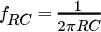
In other words, this circuit is expected not to be able to propagate signals whose frequency exceeds fRC. To increase this cut-off frequency, it is thus necessary to either reduce R or C. In the late 1990s, chip manufacturers did both.
1.1.2 The damascene architecture
Until then, the metal and dielectric material used to fabricate interconnect structures were Al and SiO2, respectively. To reduce R and C, these materials were abandoned and replaced by Cu and so-called low-K dielectric materials. The latter are SiO2 derivatives, incorporating apolar chemical species such as methyl groups to decrease their relative permittivity [LE 13]. More recently, porous variants have been introduced: the incorporation of nanosized pores in the material allowed further reduction of the K value down to 2.2 [GRI 01].
1.1.2.1 Cu as a conducting metal
Cu was selected as a replacement metal for Al because of its lower resistivity (ρCu = 1.67 μΩ · cm), but also because of its better resistance to electromigration (EM) as compared to the more conductive Ag and Au (see section 5.2.1 for more details about EM).
However, the introduction of Cu has not been straightforward. Indeed, this metal was not compatible with the process flow used to fabricate a metal level with Al. The latter is shown in Figure 1...
Table of contents
- Cover image
- Title page
- Table of Contents
- Dedication
- Copyright
- Acknowledgments
- Introduction
- 1: The Fabrication of Micro- and Nanostructures
- 2: Phase Transition: Nucleation, Growth, Aggregation and Coalescence
- 3: The Precipitation of Metals: Thin Film Electroplating and Nanoparticle Synthesis
- 4: Copper Electroplating: from Superconformal to Extreme Fill
- 5: Nucleation and Growth of Metallic Thin Films
- 6: Nucleation and Stabilization of Metallic Nanoparticles in Ionic Liquids
- Appendix 1: Demonstration of the General Expression for the Nucleation Rate
- Appendix 2: Stationary Cluster Population and Nucleation Rate
- Appendix 3: Where is the Surface of the Cluster?
- Glossary
- List of Acronyms
- Bibliography
- Index
Frequently asked questions
Yes, you can cancel anytime from the Subscription tab in your account settings on the Perlego website. Your subscription will stay active until the end of your current billing period. Learn how to cancel your subscription
No, books cannot be downloaded as external files, such as PDFs, for use outside of Perlego. However, you can download books within the Perlego app for offline reading on mobile or tablet. Learn how to download books offline
Perlego offers two plans: Essential and Complete
- Essential is ideal for learners and professionals who enjoy exploring a wide range of subjects. Access the Essential Library with 800,000+ trusted titles and best-sellers across business, personal growth, and the humanities. Includes unlimited reading time and Standard Read Aloud voice.
- Complete: Perfect for advanced learners and researchers needing full, unrestricted access. Unlock 1.5M+ books across hundreds of subjects, including academic and specialized titles. The Complete Plan also includes advanced features like Premium Read Aloud and Research Assistant.
We are an online textbook subscription service, where you can get access to an entire online library for less than the price of a single book per month. With over 1.5 million books across 990+ topics, we’ve got you covered! Learn about our mission
Look out for the read-aloud symbol on your next book to see if you can listen to it. The read-aloud tool reads text aloud for you, highlighting the text as it is being read. You can pause it, speed it up and slow it down. Learn more about Read Aloud
Yes! You can use the Perlego app on both iOS and Android devices to read anytime, anywhere — even offline. Perfect for commutes or when you’re on the go.
Please note we cannot support devices running on iOS 13 and Android 7 or earlier. Learn more about using the app
Please note we cannot support devices running on iOS 13 and Android 7 or earlier. Learn more about using the app
Yes, you can access Nucleation and Growth of Metals by Paul-Henri Haumesser in PDF and/or ePUB format, as well as other popular books in Technology & Engineering & Mining Engineering. We have over 1.5 million books available in our catalogue for you to explore.