![]()
Chapter 1
Solder Products and Soldering Process
1.1Solder Products
The broad applications of electronic products for consumer, industrial, defense, and commercial applications, etc., in the past decades have nourished the development and production of solder products. The end system of the electronic products, for instances the mobile phone, computers, audio-videos, automotive, avionic, etc., is an architect structure which is comprised of a variety of components. In brief, the frame of the component is mainly composed of chip, module, substrate, lead frame and board. The functioning of the system relies on the link of all the components facilitated by appropriate interconnects. A variety of interconnects are available in industry. These include metallic wire bond, conductive adhesive, and solder joint. Among these, the interconnect which exhibits the broadest types of products, perhaps, is the solder joint. The solder joints are in need and manufactured at the various stages of electronic packaging such as wafer level packaging, module level packaging, and system level packaging throughout the entire manufacture scheme.
A variety of solder products have been in use in industry. The selection of solder products depends on the type of electronic products and manufacturing process. The industrial solder products are produced in numerous types including solder bar, solder wire, solder preform, solder ball, solder bump, solder shot, solder powder, and solder paste. Electronic industry is one of the major industries which utilize these solder products.
Fig. 1.1.The solder ball (inset) and solder bar (upper left).
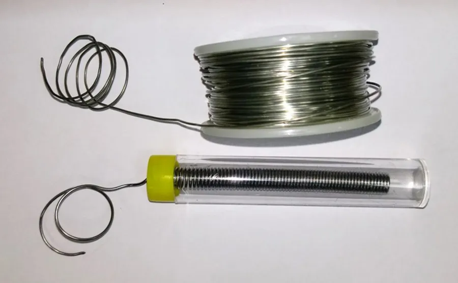
Solder anode and cathode cast is among the largest solder products in terms of dimension of solder products. Solder bar, upper left in Figure 1.1, is also a cast mainly applied as the raw material for wave soldering bath. The solder bar is available for different solder alloys. Solder wire, Figure 1.2, has been used for manual soldering such like rework. Solder alloys are generally soft and ductile which allow easy drawing. The manual soldering was conducted with the aids of flux to deoxidize and enhance solderability. The industries have also developed flux cored solder wire. The flux was filled in hollow solder wire so as to allow the convenient manual soldering process. The flux cored solder wire facilitates consistent fluxing quality of the soldering operation.
One of the major applications of solder powder is the manufacturing of solder paste, Figure 1.3. The commercial solder powder size ranges from a few to tens micrometers. Miniaturized products, for example, wearable and IOT (interconnect of things) electronics, need finer solder powders for achieving fine joint with fine pitch requirements. Solder paste is widely applied for surface mount technology (SMT) application. The flip chip solder bump may also be produced out from solder paste. One of the common practices of solder paste application is through screening printing. The solder paste is paved on the pad lands, defined by stencil, where the SMT leads of modules are to be located and joined. In some applications the via for the THT (through hole technology) process could also be filled with solder paste for joining the inserting leads. In order for enabling the convenient and uniform spread of the paste in screen printing, spherical powders are generally preferable.
Fig. 1.2.Solder wire.
Fig. 1.3.Solder paste.
Fig. 1.4.The oxide layer formed on metal surface results in large contact angle (the inner angle between the line and the surface) and thus poor solderability (left), small contact angle and thus good solderability achieved on metal surface where the oxide layer is removed with flux (right).
The solder paste is made of a complicate formula comprising flux and solder powders. It is not intended here to discuss the composition of the flux. In general, the flux contains solvent, natural (Abietic Acid) or synthetic rosin, and activators. It provides the functions of cleaning oxides or tarnishes on solder, bonding pad, and lead frame. The flux protects the cleaned metals from further oxidation during the reflow process even when the flux vaporizes. In addition, the flux atmosphere produced during reflow also facilitates the wetting of solder on bonding pad and lead frame by reducing the contact angle as delineated by Figure 1.4. The solderability will be further discussed in latter chapter. In view of the fact that the screen printing is practiced at ambient condition, solder paste is generally acquired to maintain stable properties at ambient conditions. It is desired to exhibit no significant viscosity change during long time storage or the reasonable duration of manufacturing process. The rheology, powder size, and metal load are all of importance when formulating the solder paste. For the reliability concern of electronic products, the solder pastes are mostly halogen free and with non-clean residue. Solder pastes are available in different packages such as bottle, syringe (Figure 1.3), etc., for the need of various manufacturing processes. Almost all the SMT packaging process will need solder pastes for mounting of silicon chip or modules. Solder pastes have also been applied in chip level packaging, for example, the manufacturing of solder bump with screen printing of solder paste, Figure 1.5. Solder paste has also been widely applied for mounting of leaded modules such as CSP (chip scale package), PLCC (plastic leaded chip carrier), QFP (quad flat package), etc. The modern types of packaging such as POP (package on package) also applied solder paste for 3D stacking of modules.
Fig. 1.5.Manufacturing of solder bump on silicon chip with solder paste screening printing process. The enlarged image shows the solder powders filled in the opening defined photoresist.
The electronic products which do not exhibit conformal plane of interconnects or have discrete interconnects may need to apply solder preform for the solder joints. The ductile character of solder allows relatively easy fabrication of solder preform through rolling, stamping, etc. Solder preform, is available in various shapes such as coin (Figure 1.6), ring, rectangle, washer, pellet, or ribbon. It could also be made customized. The designed shape and dimension of the solder preform allows the precise control of the solder volume when necessary and the flexible manufacturing application. Solder preform is also available with flux coating.
The packaged modules need to mount on PC board. All the modules are integrated on a board, for example, the PC board of a computer. The variety of components/modules on a PC board as shown in Figure 1.7(a) are mounted with solder joints. The solder joints provide the mechanical strength as well as electrical transport. On the module level packaging, the components may be mounted through surface mount technology (SMT) by reflow of solder paste (front of Figure 1.7(b)). The solder paste was paved on the land pad for lead frame attachment by screen printing. The solder melts during reflow and fixes the component by joining the lead frame and the board metallization pad when solidified. The SMT may also join the component via solder ball (center of Figure 1.7(b)) which were arranged underneath the ball grid array (BGA) substrate to join the BGA module on PC board. The solder balls bond the metallization on both the BGA substrate, for example Cu/Ni/Au, and the board, for example, OSP (organic solder protective)/Cu. A chip with high power generation during functioning is seen covered by a heat dissipation aluminum fin module (central module on Figure 1.7(a); fin substrate opened to reveal the chip in Figure 1.7(c)). An even higher power module would further incorporate cooling fan to expedite heat dissipation (upper right of Figure 1.7(a)). The heat generated from the high power chip is dissipated mainly through the heat dissipation fin structure bridged by thermal grease (the broken light spread on the bottom of the opened fin module). A high thermal conductive metal lead may be applied on top of the high power large die (Figure 1.7(d)) before incorporating with the fan module (center right of Figure 1.7(a)). The high power chip is mounted on top of the BGA substrate via flip chip technology because of the need of large number of I/Os. Besides the components with high pin counts (high I/Os) there are components with only a few number of I/Os like the passive components shown in the left front of Figure 1.7(e). The passive components with low pin counts are joined on the board via through hole technology (THT). The THT utilizes the wave soldering process. The leads of the loosely fixed component inserted in the via are passed through the liquid solder wave. The solder bonds the through-via metallization plating and the pre-inserted leads when solidified.
Fig. 1.6.Solder preform coins.
Fig. 1.7.(a) The PC board contains various types of electronic products. (b) The forefront components in the enlarged image are mounted with SMT technology which adopts solder paste for reflow. The center component is mounted with BGA technology which uses solder balls (invisible underneath the BGA substrate). (c) The chip underneath the heat dissipation fin structure is mounted on a BGA module with flip chip bonding technology which adopts solder bumps. (d) The higher power chip incorporated with thermal conductive metal lid on top to facilitate heat dissipation. (e) The passive component (inset) with two pins is fixed on the board with through-hole technology (THT) which utilizes wave soldering process.
As mentioned above, the solder joint may be produced through different processes depending on the level of packaging and the types of package. From this perspective, the solder joints are produced in various types. The level of packaging can be categorized into chip level (or wafer level), module level, and board level (or system level). On the chip level, the die may need to bond to lead frame or appropriate substrate. The major technologies in industrial practice for die bonding/interconnecting include wire bonding, tape automated bonding (TAB), and flip chip bonding. Among these, the flip chip adopted solder bumps, Figure 1.8, are produced on silicon chip during the wafer-level process. The entire flip chip solder bump structure may consist of under bump metallurgy (UBM; or ball limiting metallurgy, BLM) and solder bump. The UBM starting from the terminal (e.g., Al) of the chip followed by adhesive layer (e.g., Ti/Cu), barrier layer (e.g., Ni), and wetting layer (e.g., Au). The solder deposit may be produced on top of UBM by electroplating (Figure 1.8(a)) followed by reflow to form spherical solder bump (Figure 1.8(b)). The solder may also be produced by screen printing, (Figure 1.5), using solder paste, followed by reflow. Both electroplating and screen printing processes need to define the opening for solder bump with lithography technology. The example of process flow is given in Figure 1.9. The photolithography defines the bump opening. The metallization exposed in the opening area are deposited sequentially with electroless nickel and solder plating in this example sketch. The mushroom shaped solder plating will be reflowed to form aspherical solder bump, and the photoresist mask is stripped off. The so...