Technology & Engineering
Hall Effect
The Hall Effect is a phenomenon in physics where a voltage difference is created across a conductor transverse to the electric current and a magnetic field. This effect is used in various technologies, such as sensors and electronic devices, to measure magnetic fields, detect current, and determine the type of charge carriers in a material.
Written by Perlego with AI-assistance
Related key terms
1 of 5
8 Key excerpts on "Hall Effect"
 eBook - ePub
- David Nyce(Author)
- 2023(Publication Date)
- CRC Press(Publisher)
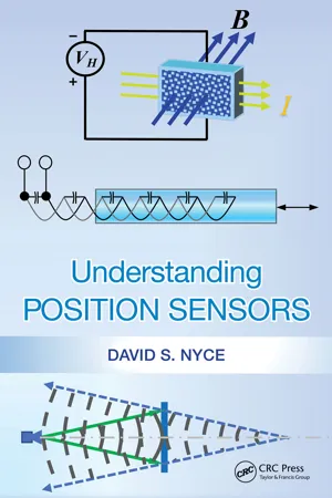
With commercially available Hall devices, the conductor (semiconductor) dimension is already known by the manufacturer, and the sensitivity is specified for the particular model. In this case, formula 10.1 can be simplified to:V = K B I(10.2)where K is the sensitivity factor, usually in volts per gauss or volts per milli tesla (milli tesla is abbreviated as mT), that is specified by the manufacturer. 1 tesla = 10,000 gauss.10.3 History of the Hall Effect
In 1879 at Johns Hopkins University, physicist Dr. Edwin H. Hall discovered the effect that now bears his name [2, p 473; 3, p 1]. He found that a voltage potential appears across a conductor when a magnetic field is applied at right angles to the flow of an electric current in the conductor. This voltage potential is called the Hall voltage (refer back to Figure 10.1 ). The Hall Effect has been used to develop sensing elements that measure the strength and polarity of a magnetic field. These magnetic field sensors have been further developed into position sensors, where change in the position of a magnet attached to a target results in change in the magnetic flux density at the location of the Hall device. (A Hall Effect-based sensing element is often called a Hall device.)Although discovered in the late nineteenth century, the Hall Effect had little commercial use until the 1950s when development of semiconductor compounds led to the first useful Hall Effect laboratory instruments. The use of a Hall Effect sensor allowed the measurement of a static magnetic field, which was not possible with the coil assemblies previously used for magnetic field measurement (coils can sense only alternating fields). Once the Hall Effect sensor and some signal conditioning electronics were incorporated into a single integrated circuit in the 1960s, many applications became practical. Most of the early sensing applications were for switch-type sensors. These included keyboards, joysticks, and other industrial and commercial products.The presence of an offset voltage and of temperature sensitivity noticeably limited the performance of single-element Hall Effect sensors. To obtain a lower offset voltage and lower temperature sensitivity of the offset voltage, dual elements were used as a partial solution. This was followed by the development of quad elements in a bridge configuration. Most present-day Hall devices are of a bridge configuration. The resulting capability for operating over a wider temperature range made automotive sensors and control systems possible. Further integration of the circuitry and use of the bridge configuration improved the performance of the switch-type devices and also made linear sensors practical. Since the output voltage from the Hall device is very low, chopper-stabilized amplifiers were integrated in order to remove any offset voltage error that originated in the earlier DC amplifiers. A later method, also used to eliminate offset errors, involves constantly switching the polarity of the input current to the Hall device, thereby producing an AC signal and taking away the drift-prone DC bias by using an AC amplifier. eBook - ePub
Quantum Mechanics
Axiomatic Theory with Modern Applications
- Nelson Bolivar, Gabriel Abellán(Authors)
- 2018(Publication Date)
- Apple Academic Press(Publisher)
chapter 15Introduction to Quantum Hall Effect
In 1879, Edwin Hall [137], observed for the first time an effect on some materials that today is called Hall Effect. This essentially consists in establishing a potential difference, called Hall VHpotential, on the opposite faces of a metal sample and obtain a separation between holes and electrons.15.1 Classical Hall EffectThe Hall Effect is observed in experimentally in thin bands of conductive or semiconductor metal material, driven by an intensity current I subjected to the action of a magnetic field B . To describe the phenomenon we assume the current to be on the x axis and suppose a uniform magnetic field along the z axis: under these conditions there is a potential difference transverse, or Hall voltage VStarting from this tension, it is possible to determine the cross resistance, which is the Hall resistance, that is equal to:H, between the lateral surfaces of the conductor.(15.1)R H==V HIBn eewhere e is the charge of the electron and nethe density of the charge carriers. What makes this effect important is that from the applied VHvoltage it is possible to determine the charge carrier sign. Another important aspect is that the cross‐resistance RH, although having resistance dimensions, does not correspond to the strength resistance of the material. It is also independent of the geometry of the system and is proportional to the intensity of the applied magnetic field.Figure 15.1: Schematics of the Hall device.15.1.1 The Drude Model
To describe the quantum case it is important first to define some fundamental quantities such as longitudinal resistivity and Hall conductivity.Let us consider a two‐dimensional electronic system: it is observed that in the absence of a magnetic field, the current induced by the electric field E is parallel to the same field and the current density is equal to j = σE where σ is the conductivity of the material. In the presence of a magnetic field B , a transverse current density is created which tends to accumulate charges on the edges of the sample until the balance is reached between the electric force generated by this charge distribution and the Lorentz force generated by the magnetic field. In the ideal case only the B perpendicular component of the 2-d system influences the electronic motion, while only the electric field component lying on the plane of the system has effects on the current. In this case we can then write the relation between the current and the field E by introducing the two‐dimensional current density j and the conductivity tensor σ
- J Suchet(Author)
- 2012(Publication Date)
- Academic Press(Publisher)
Let us assume the existence of an induction B along the first, and a current / along the second. An electrical field E H then appears along the third: E H = -gradK H = RBI/ac (10.1) This is the Hall Effect, and grad V H refers to the potential gradient along the z direction; R is a coefficient independent of B or /, called the Hall co-efficient. In a homogeneous material, the field E H produces a voltage V H , known as the Hall voltage, and in a diamagnetic material the induction B is equal to the external magnetic field H, so that V H = -RHI/a (10.2) where a is the thickness of the sample in the direction of the applied magnetic field. The origin of the Hall Effect lies in the force to which a moving charged particle is subject in a magnetic field (Lorentz force). A curve is produced 299 300 Hall Magnetoelectric Effects in its rectilinear trajectory by the field H, so that the charges gather on the sides of the sample, until the effect of the lateral electrical field thus set up counter-balances the deviation caused by the field H (Fig. 10.1). The trace of the electrical equipotential surfaces on the plane of Fig. 10.2 is thus no longer perpendicular to the direction of the current, but revolves by a certain angle, generally small: 0 = tan 0 = E H /E y (10.3) where E y is the electrical field responsible for the passage of the current /. Taking (10.1) into account, there occurs, in a diamagnetic material 0 ~ RHa (10.4) The force to which a moving particle is subject when equilibrium is attained can therefore be expressed in two different ways. First, Eq. (10.1) gives: eE H = eRHI/ac (10.5) Second, the force eE z caused by the lateral electrical fielJ exactly counter-balances the effect of the Lorentz forces, which can be expressed here as: eE z = eHI/Neac (10.6) where Wis the carrier density. eBook - ePub
- John R. Brauer(Author)
- 2014(Publication Date)
- Wiley-IEEE Press(Publisher)
y direction is:(10.1)wheredyis the terminal (electrode) spacing shown in Figure 10.2 , which also shows the current densityJxflowing in the x direction, along with the flux densityBz. The Hall voltage is developed because the current experiences the Lorentz force of Chapter 2. It can be shown that the Hall electric field E in volts per meter balances the motional electric field of (2.36) [1].Figure 10.2 Hall Effect voltage in a narrow semiconductor bar.The Hall coefficientkHin (10.1 ) can be shown for a narrow bar withdxdyto equal approximately [1]:(10.2)where n is the electron concentration in electrons per cubic meter and e is the charge on an electron = 1.602E–19 C. The electron concentration varies with the semiconductor material used. Typically, silicon is used, because it is so widely available, thermally stable, inexpensive, and has conductivity in the semiconductor range. In fact, many Hall sensors are built within CMOS or other integrated silicon circuits. The semiconductor range of conductivity is within several orders of magnitude of 1 S/m, and can be varied by doping with impurities. If doped so as to contain holes, the Hall constant of (10.2 ) becomes:(10.3)where p is the hole concentration in holes per cubic meter.Practical Hall sensors often have many large electrodes and a wide range of geometries, which can make the accuracy of (10.1 ) poor. To analyze a wide range of geometries and materials, a numerical technique is required that will solve for current flow in Hall sensors [2].10.2 Hall Effect CONDUCTIVITY TENSORCurrent flow is governed by Ohm's law for fields given in Chapter 2. When conductivity σ eBook - PDF
- Ralph Dougherty, J. Daniel Kimel(Authors)
- 2012(Publication Date)
- CRC Press(Publisher)
* The Hall Effect is the development of a voltage in the y axis when there is a current flowing in the x axis of the magnetoresistance experiment illustrated in Figure 9.1. Hall Effect measurements of magnetic field strength were, for a long period, the only reliable method for obtaining magnetic field data. There is a large supporting literature both scientific and commercial. Studies of pure magnetoresistance in polycrystalline metal samples have not, in comparison received much attention, though a small number of papers on the angular anisotropy of magnetoresistance are very informative. * P. I. Kapitza went on from his studies of magnetoresistance to discover superfluidity in helium-4, 4 He, in 1937. He received the Nobel Prize in 1978 for superfluidity, 50 years after his investigation of magnetoresistance. 4 2 1 B z y x I 3 FIGURE 9.2 Standard electrical connection post configuration on a Hall bar. (–) B (+) (+) (+) (+) (+) (+) (+) (+) I (–) (–) (–) (–) (–) z y x (–) (–) FIGURE 9.1 Classical schematic of electron trajectory in the Hall Effect for a pure metal; current and fields follow physics conventions. 79 Magnetoresistance HALL COEFFICIENT Equation (9.2) gives the definition of the Hall coefficient. It is the ratio of the applied electric field on the x -axis to the product of the magnetic flux density times the Hall current density on the y -axis, j y . = -R E Bj H x y (9.2) R H is the conventional label for the Hall coefficient. ρ xy conventionally designates Hall resistivity. Positive Hall coefficients occur significantly less often than negative Hall coef-ficients. Materials with positive Hall coefficients are found in a few elemental metals and p -type semiconductors. Generally, materials with positive Hall coefficients are not classed as good conductors. For example, the semiconductor, diamond lattice tin, * has a positive Hall coefficient. This crystalline form of tin is never involved in superconductivity. eBook - PDF
- Wolfgang Göpel, Joachim Hesse, J. N. Zemel, Wolfgang Göpel, Joachim Hesse, J. N. Zemel(Authors)
- 2008(Publication Date)
- Wiley-VCH(Publisher)
The exploitation of this effect in sensors has only been worthwhile since the development of III/V semiconductors. A free charge carrier in a semiconductor is deflected by the Lorentz force which acts perpen- dicular to the direction of the motion and the magnetic flux density. The charge carrier even- 36 2 Physical PrincipIes tually collides with the crystal lattice and the rotation of the current direction occurs which results in an increase in the length of the path of the current flow. This increase in the path length produces an increase in the resistivity of the material, magnetoresistance, which is the physical basis of a family of magnetic sensors. If a very long strip of strongly extrinsic and homogeneous semiconductor material carries a current, I,, in the x direction and when the strip plane is in the xy plane then an applied field in the z direction, manifested as a flux density, B,, produces a transverse electric field in the JJ direction, the Hall field (see Figure 2-4). Figure 2-4. Schematic diagram of Hall Effect. The Hall voltage, U,, is approximately proportional to the product of the flux density perpendicular to the strip plane, B,, and the current I,. U, - B, . I , . The theoretical basis of the Hall Effect - that is, the effect of the Lorentz force on the charge-carrier transport phenomenon occuring in condensed matter - is well described in Chapter 3. 2.3 Magnetostriction and Magnetoelastic Effects In 1842 Joule observed that when a magnetic rod was subjected to a longitudinal magnetic field then the length of the rod changed. This longitudinal magnetostrictive (change of dimen- sions due to effect of the magnetic field) phenomenon is called the Joule effect [3]. If there is an increase in length in the longitudinal direction then a decrease in dimensions takes place in the transverse direction and, in general, a change in the volume of the material occurs.
- Winncy Y. Du(Author)
- 2014(Publication Date)
- CRC Press(Publisher)
The charge then builds up and forms a measurable voltage between the two sides of the conductor (see Figure 5.1). This voltage is called Hall voltage , V H , named after Edwin Hall who discovered this phenomenon in 1879 [1]. V H can be described by V IB qN t H C h = (5.1) x z y I B l w t h V H I FIGURE 5.1 Hall Effect. T ABLE 5.1 Ma gnetic Field Detection Ranges of Inductive and Magnetic Sensors Detectable Magnetic Field (Tesla) Inducti ve/Magnetic Sensors 10 unif02d 14 10 unif02d 10 10 unif02d 6 10 unif02d 2 10 2 Coil sensors Fluxgate sensors Hall ef fect sensors Magnetoresisti ve sensors Magnetoimpedence sensors Nuclear magnetic resonance sensors Magneto-optical sensors SQUIDs 225 Magnetic Sensors where I is the current (in A), B is the magnetic field density (in T), q is the charge of an electron (1.602 × 10 − 19 C), N C is the number of charge carriers per cubic meter (in m − 3 , called Charge Carrier Density ), and t h is the thickness of the conductor (in m). The Hall voltage V H is directly proportional to the current I and the magnetic field B , and inversely proportional to the thickness of the conductor t h . If the applied magnetic field is along the z -axis, perpendicular to the current in the x -axis, and then the Hall voltage is measured in the y -axis. The inverse of qN is called Hall coefficient , denoted as C H (in m 3 ⋅ C − 1 or m 3 ⋅ A − 1 ⋅ s − 1 ): C qN H C = 1 (5.2) EXAMPLE 5.1 In a typical Hall sensor application, I = 1 mA, B = 0.1 T, t h = 10 μ m, and C H = 0.006 m 3 ⋅ C − 1 (or m 3 ⋅ A − 1 ⋅ s − 1 ). Find the Hall voltage V H . S OLUTION Apply Equation 5.1: V C t IB H H h = = ⋅ × × = ---0 006 10 10 1 10 0 1 0 06 6 3 . ( )( . ) . m C m A T V or60 mV 3 1 Equation 5.1 shows that the Hall voltage does not depend on the strip width, w , and the length, l , but its thickness, t h . A thinner or smaller t h provides a larger Hall voltage. eBook - PDF
Experiments And Demonstrations In Physics: Bar-ilan Physics Laboratory (2nd Edition)
Bar-Ilan Physics Laboratory
- Yaakov Kraftmakher(Author)
- 2014(Publication Date)
- World Scientific(Publisher)
The force F on a charge q (Lorentz’s force) is given by F = q E + q v × B , (1) where E is the electric field, and v is the velocity of the charge. Fig. 1. Schematic for calculating the Hall’s effect. Due to the magnetic field, the carriers are deflected perpendicular to their velocity and the magnetic field. In the case considered, the vector B is perpendicular to the vector v . The deflected carriers produce a transverse electric field E y called the Hall field . In the steady state, this field gives rise to an electric force that just cancels the force due to the magnetic field: qE y = qv x B z . (2) The Hall field can be expressed as E y = j x B z / nq = R H j x B z , (3) where n is the concentration of the carriers, and R H is called the Hall coefficient . In semiconductors, it is given by R H = –1/ ne for electrons and 1/ pe for holes, where n and p are their concentrations. From the measurements, the Hall coefficient and thus the concentration of free carriers are available. Furthermore, the sign of the Hall coefficient gives the sign of the carrier charge. From measurements of the conductivity and Hall’s effect, basic characteristics of a semiconductor are available, the carrier 7.2. Hall’s effect 453 output Hall probe potentiometer I data-acquisition system input A output Hall probe current (mA) Hall voltage (V) 1 2 concentration and mobility. With Hall’s effect, Klein (1987) demonstrated the drift velocity in metals. Armentrout (1990) observed the effect in copper. In the experiment, we use a commercial Hall’s probe. The Signal generator feeds the probe, and the Voltage sensor measures the Hall voltage generated by the probe (Fig. 2). The feeding DC current is measured as the Output current . The I – V characteristics of the probe are determined at room temperature and when the probe is immersed in liquid nitrogen. In both cases, the probe is positioned between poles of a permanent magnet providing a field of 0.2 T.
Index pages curate the most relevant extracts from our library of academic textbooks. They’ve been created using an in-house natural language model (NLM), each adding context and meaning to key research topics.