- 224 pages
- English
- ePUB (mobile friendly)
- Available on iOS & Android
eBook - ePub
Power Electronics
About this book
Since its inception, the Tutorial Guides in Electronic Engineering series has met with great success among both instructors and students. Designed for first and second year undergraduate courses, each text provides a concise list of objectives at the beginning of each chapter, key definitions and formulas highlighted in margin notes, and references to other texts in the series.This volume introduces the subject of power electronics. Giving relatively little consideration to device physics, the author first discusses the major power electronic devices and their characteristics, then focuses on the systems aspects of power electronics and on the range and diversity of applications. Several case studies, covering topics from high-voltage DC transmission to the development of a controller for domestic appliances, help place the material into a practical context. Each chapter also includes a number of worked examples for reinforcement, which are in turn supported by copious illustrations and end-of-chapter exercises.
Trusted by 375,005 students
Access to over 1.5 million titles for a fair monthly price.
Study more efficiently using our study tools.
Information
1
Power semiconductors
Objectives
□ To introduce the major power electronic devices.
□ To define their operating regimes and modes of operation.
□ To establish their ratings.
□ To consider losses and heat transfer properties.
□ To examine means of protection.
An intrinsic semiconductor is defined as being a material having a resistivity which lies between that of insulators and conductors and which decreases with increasing temperature. The principal semiconductor material used for power electronic devices is silicon, a member of Group IV of the periodic table elements which means it has four electrons in its outer orbit.
If an element of Group V, such as phosphorus, with five electrons in its outer orbit is added to the silicon, each phosphorus atom forms a covalent bond within the silicon lattice, leaving a loosely bound electron. The presence of these additional electrons greatly increases the conductivity of the silicon and a material doped in this way is referred to as an n-type semiconductor.
By introducing an element from Group III as impurity, a vacant bonding location or hole is introduced into the lattice. This hole may be considered to be mobile as it can be filled by an adjacent electron, which in its turn leaves a hole behind. Holes can be thought of as carriers of positive charge and a semiconductor doped by a Group III impurity is referred to as a p-type semiconductor.
The extra, mobile electrons introduced by doping into the n-type material and the equivalent holes in the p-type material are referred to as the majority carriers. In an n-type material there is a small population of holes and in a p-type material a small population of electrons.
These are called the minority carriers.
Diode
The semiconductor junction diode shown in Fig. 1.1 is the simplest semiconductor device used in power electronics. With no external applied voltage the redistribution of charges in the region of the junction between the p-type and n-type materials results in an equilibrium condition in which a potential barrier is established across a narrow region depleted of charge carriers on each side of the junction. This equilibrium may be disturbed by the application of an external applied voltage of either polarity.
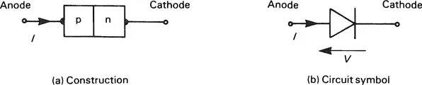
Fig. 1.1 The diode.
Ghandi, S.K. (1977).
Semiconductor Power Devices.
Wiley Interscience.
Sparkes, J.
Semiconductor Devices. (1987).
Van Nostrand Reinhold.
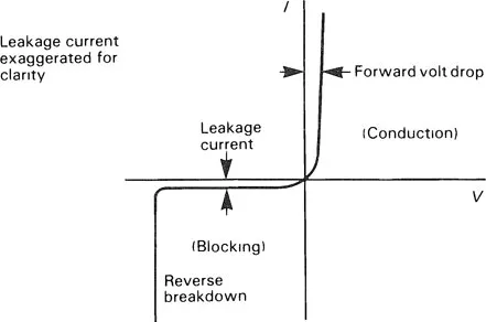
Fig. 1.2 Diagrammatic representation of the diode static characteristic. (Note: forward and reverse voltage scales are unequal. The forward voltage drop is of the order of 1 V while the reverse breakdown voltage varies from a few tens of volts to several thousand.)
The region over which the potential barrier exists is known as the depletion or transition layer.
If a reverse voltage – cathode positive with respect to anode – is applied, the electric field at the junction is reinforced, increasing the height of the potential barrier and increasing the energy required by a majority carrier to cross this barrier. The resulting small reverse leakage current shown in the diode static characteristic of Fig. 1.2 is due to the flow of minority carriers across the junction. The magnitude of the reverse leakage current increases with temperature because the number of minority carriers available increases with the temperature of the material.
The magnitude of the reverse leakage current can vary from a few picoamperes for an integrated circuit diode to a few milliamperes for a power diode capable of carrying several thousand amperes in the forward...
Table of contents
- Cover
- Half Title
- Title Page
- Copyright Page
- Table of Contents
- Preface
- 1 Power semiconductors
- 2 Converters
- 3 DC choppers, inverters and cycloconverters
- 4 Applications I – drives
- 5 Applications II – power supplies
- 6 Applications III
- 7 Harmonics and interference
- Appendix A Three-phase systems
- Appendix B Fourier analysis
- Answers to problems
- Index
Frequently asked questions
Yes, you can cancel anytime from the Subscription tab in your account settings on the Perlego website. Your subscription will stay active until the end of your current billing period. Learn how to cancel your subscription
No, books cannot be downloaded as external files, such as PDFs, for use outside of Perlego. However, you can download books within the Perlego app for offline reading on mobile or tablet. Learn how to download books offline
Perlego offers two plans: Essential and Complete
- Essential is ideal for learners and professionals who enjoy exploring a wide range of subjects. Access the Essential Library with 800,000+ trusted titles and best-sellers across business, personal growth, and the humanities. Includes unlimited reading time and Standard Read Aloud voice.
- Complete: Perfect for advanced learners and researchers needing full, unrestricted access. Unlock 1.5M+ books across hundreds of subjects, including academic and specialized titles. The Complete Plan also includes advanced features like Premium Read Aloud and Research Assistant.
We are an online textbook subscription service, where you can get access to an entire online library for less than the price of a single book per month. With over 1.5 million books across 990+ topics, we’ve got you covered! Learn about our mission
Look out for the read-aloud symbol on your next book to see if you can listen to it. The read-aloud tool reads text aloud for you, highlighting the text as it is being read. You can pause it, speed it up and slow it down. Learn more about Read Aloud
Yes! You can use the Perlego app on both iOS and Android devices to read anytime, anywhere — even offline. Perfect for commutes or when you’re on the go.
Please note we cannot support devices running on iOS 13 and Android 7 or earlier. Learn more about using the app
Please note we cannot support devices running on iOS 13 and Android 7 or earlier. Learn more about using the app
Yes, you can access Power Electronics by David Allan Bradley in PDF and/or ePUB format, as well as other popular books in Technology & Engineering & Civil Engineering. We have over 1.5 million books available in our catalogue for you to explore.