![]()
Chapter 1
Chemistry in the “Front End of the Line” (FEOL): Deposits, Gate Stacks, Epitaxy and Contacts
1.1. Introduction
The manufacturing of a transistor involves several hundred production and control stages and is a process that takes several weeks, generally between four and twelve depending on the complexity of the electronic component. Production is considered to be either “front end” or “back end”.
A “front end” plant will produce a component consisting of between hundreds of millions and several billion transistors, all interconnected via different stages. Today the most advanced technologies with 20 nm nodes use between eleven and thirteen metal levels to interconnect several billion transistors by means of a specific map that is determined by the feature of the component. The component is tested and the functional chips are identified and selected in order to calculate what is known as the yield, that is the number of chips made to specifications versus the total number made. A “back end” plant will receive the “front end” components and finalize the packaging through a second pathway and specific processes. Tests then guarantee the reliability of the component, generally over a period of 10–20 years.
In the “front end” plant, the manufacturing of the component is itself divided into two main sectors: first, the “front end of the line” (FEOL), which could be considered as the technological heart of the operation. It involves the extreme optimization of each individual transistor: dimensioning, type (N or P), arrangement, characteristic (high performance or low consumption, for example) and application (logic, analog, etc.). The second area of manufacturing is known as the “back-end of the line” (BEOL) and will be explained in Chapter 2 of this book, simplified, its aim is to optimize the interconnection of the individual transistors made by the FEOL sector.
This chapter focuses on the FEOL sector: it can be divided into several subsectors of activity; through processes, we will successively list zones for deposition, mechanical–chemical polishing, dry and wet etching, surface preparation/cleaning, doping or lithography. For each technological node, there are groups of experts aiming to define the specifications required for these different processes, in order to obtain the desired features for various applications. This is done by the international group, International Technology Roadmap for Semiconductors (ITRS) [ITR 12].
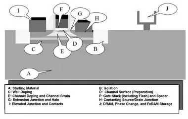
A modern transistor must address the various technological aspects that are shown in Figure 1.1. The challenges concern the starting material “A” (generally silicon, eventually modified to a version called silicon on insulator (SOI) corresponding to an ingenious Si/SiO2/Si stack where the highest active layer of silicon is isolated from the substrate by an embedded layer of oxide), the insulation between the transistors (B), the determination of the dopant profiles (target addressed by points C, E and G), the gate stack (D and F), the contact zones of the gate as well as the “Source” and “Drain” zones of the transistor (H and I), etc. [ITR 11].
This chapter describes three important elements. In Figure 1.1, these are described mainly by points F, H and I, and somewhat by D and E as well. First, the chemistry involved in the gate stack is described as this is directly related to a fine tuning of the transistor: the optimization of the gate insulator and the gate itself. The choice of the chemical precursors is of key importance. Next, crystalline heterostructures (based on SiGe in particular) are explained and the involvement of the precursors, temperature, pressure and surface preparation is detailed. Finally, the chemistry involved to address efficient contacts is also precisely described.
Figure 1.1. The challenges of the “front end of the line” as defined by the ITRS [ITR 11]
1.2. Arrangement of the gate
1.2.1. Generalities
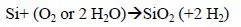
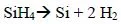
After the discovery of the planar structure in the 1960s, for a long time the gate stack of the metal oxide semiconductor (MOS) transistors was made of a silicon (SiO2) insulator covered by a gate for the channel control (itself made of N and P doped polycrystalline silicon). Looking at the chemical processes used in the production of this stack, first a thermal oxidation of the silicon takes place in the heat treatment furnace containing several tens of wafers (reaction [1.1]). Then the silicon gate is deposited by chemical deposition in the vapor phase low pressure chemical vapor deposition (LPCVD) from silane in a furnace under vacuum (reaction [1.2]).
For dimensions of about 0.18 μm and smaller, additional constraints arose: the continuation of transistor size scaling fixed the thickness of the insulation gate (Moore’s Law) and while the current tunnel through the oxide increased drastically, the boron doping diffused from the P-type metal-oxide semiconductor (PMOS) side through the gate insulator to the transistor’s channel. This chapter will explain how scientists first improved the properties of the silicon oxide, before introducing into the 45 to 28 nm nodes an innovation that would replace a large part of SiO2 by a high-permittivity insulator, known as “High K”: by depositing a greater thickness of a material with a higher permittivity, the leakage current is indeed reduced without adversely affecting the capacitive coupling. To guarantee a greater physicochemical compatibility with the High K material as well as an optimal capacitive coupling, the second major innovation was to deposit a metal gate, rather than a gate made from doped polycrystalline silicon. The latter had the disadvantage of having a slightly depleted interface doping, adding a parasitic capacity, which adversely affected the transistor’s performance. In this section, the chemical mechanisms that come into play inside the fine layers of the gate stacks will be defined as well as the precursors used for depositing the films in the manufacturing environment. The motivation behind the choice of the High K material and the interaction with its environment will only be described briefly (for more information, the reader may refer to review papers about this topic) [WIL 01, LOC 06, CHO 11].
1.2.2. Silicon nitriding processes
1.2.2.1. Thermal nitridation
In the history of the technological breakthroughs in this field, the first requirement was to increase the resistance of the silicon oxide to electrical tension (its reliability) and against the diffusion of the boron through the insulator. Before the 90 nm nodes, boron diffusion was controlled by an optimization of the implantation conditions as well as by the activation annealing of the polycrystalline silicon gate and junctions. Processes used to increase the reliability of the Si/SiO2 interface were investigated by introducing into the 2–3 nm oxide layers a very specific quantity of nitrogen. Experiments were first conducted by annealing silicon oxide in the presence of NH3, thus nitriding the oxide surface by optimizing the temperature of the process; however, the presence of reducing species resulting from the thermal decomposition of NH3 at high temperatures caused the apparition of electrical traps in the silica. This disturbance was resolved by carrying out complex reoxidizing steps on the nitrided oxide, thus increasing the difficulties for controlling the process.
Next, scientists introduced nitriding molecules that contained no hydrogen. The first attempts were carried out with N2O; however, it appeared that its complex decomposition involves the nitridation/oxidation of the interface, giving a Si–N–O bonding state, which is difficult to control uniformly over a batch of wafers [HEG 97]. By identifying that the main product of N2O decomposition was, in fact, nitrous oxide (NO), it seemed easier to introduce it directly into the annealing furnace. As the diffusivity of the NO molecule is dependent on the insulator’s growth conditions (and its stress) [SAG 96], the annealing process was optimized in order to obtain the necessary nitrogen concentration in the internal interface, depending on the silicon’s thickness. In addition, the bonds formed at the interface were of the Si–N type [HEG 97] and so by lightly reoxidizing it, the nitrogen was then in an environment of the same type as that formed by treatment with N2O, as shown by X-ray photoelectron spectroscopy (XPS) [HAL 98]. With this sort of process, approximately 0.1% nitrogen may be obtained in an optimal chemical environment [WIL 01], that is when conditions lead to the improvement of the interface’s characteristics without degrading any other properties of the transistor, such as mobility and leakage current.
1.2.2.2. Plasma nitridation
From the 90 nm technological nodes up to the advent of High K materials, a more efficient nitridation process was developed, which granted an increase in permittivity by nitriding the silica to the core. It improved the balance in the compromise between the electric thickness of the insulator (Equivalent Oxide Thickness (EOT)) and its leakage current, since permittivity increases with nitrogen incorporation, while providing a more efficient barrier to the diffusion of the boron. As the nitridation process in the presence of NO only allowed a reduced amount of nitrogen, approximately 1 × 10¹³ atm/cm2 at the Si/SiO2 interface, a new insulator-nitriding technology was required. It needed to be able to introduce a given percentage of nitrogen (between six to 15% depending on the devices) while preserving the silicon interface from nitridation for the reasons explained previously (degradation of transistor properties). The new process uses a low-energy nitrogen plasma (in the order of 1 eV), allowing nitrogen implantation in the surface and the volume of the 1.5 to 2.5 nm-thick oxide layers. The experimental procedure for this process is extensively documented [CUB 04]: the nitriding plasma first incorporates the nitrogen into the silicon oxide in the form of three Si–N bonds and unstable Si–N=O complexes. The latter are then removed by lightly oxidizing annealing, which reorganizes the Si/SiO2 interface. This must be achieved without exposure to air and so is carried out in a single-wafer treatment system that contains the nitriding plasma reactor as well as the annealing reactor. Otherwise, non-reproducible exposure to the atmosphere gives way to a reaction of non-stabilized nitrogen atoms to form N2O or NO [CUB 04]. This technology did not evolve until 40 nm nodes for the low-power technologies. To scale further electrical oxide thickness while keeping a low gate leakage current, High K/metal stacks were introduced from the 45 nm nodes for microprocessor technologies (high performance) and from the 32 nm nodes for the “low-power” technologies.
1.2.3. The introduction of the High K/metal gate stacks
1.2.3.1. The choice of High K materials in a conventional process
The selection of the best High K material for use as an insulation gate was the subject of intensive sampling by the end of the 1990s. The principal criteria of success being, besides a sufficiently high pe...