The large scale integration and planar scaling of individual system chips is reaching an expensive limit. If individual chips now, and later terrabyte memory blocks, memory macros, and processing cores, can be tightly linked in optimally designed and processed small footprint vertical stacks, then performance can be increased, power reduced and cost contained. This book reviews for the electronics industry engineer, professional and student the critical areas of development for 3D vertical memory chips including: gate-all-around and junction-less nanowire memories, stacked thin film and double gate memories,Ā terrabit vertical channel and vertical gate stacked NAND flash, large scale stacking ofĀ Resistance RAM cross-point arrays, and 2.5D/3D stacking of memory and processor chips with through-silicon-viaĀ connections now and remote links later.
Key features:
Presents a review of the status and trends in 3-dimensional vertical memory chip technologies.
Extensively reviews advanced vertical memory chip technology and development
Explores technology process routes and 3D chip integration in a single reference
Frequently asked questions
Yes, you can cancel anytime from the Subscription tab in your account settings on the Perlego website. Your subscription will stay active until the end of your current billing period. Learn how to cancel your subscription.
No, books cannot be downloaded as external files, such as PDFs, for use outside of Perlego. However, you can download books within the Perlego app for offline reading on mobile or tablet. Learn more here.
Perlego offers two plans: Essential and Complete
Essential is ideal for learners and professionals who enjoy exploring a wide range of subjects. Access the Essential Library with 800,000+ trusted titles and best-sellers across business, personal growth, and the humanities. Includes unlimited reading time and Standard Read Aloud voice.
Complete: Perfect for advanced learners and researchers needing full, unrestricted access. Unlock 1.4M+ books across hundreds of subjects, including academic and specialized titles. The Complete Plan also includes advanced features like Premium Read Aloud and Research Assistant.
Both plans are available with monthly, semester, or annual billing cycles.
We are an online textbook subscription service, where you can get access to an entire online library for less than the price of a single book per month. With over 1 million books across 1000+ topics, weāve got you covered! Learn more here.
Look out for the read-aloud symbol on your next book to see if you can listen to it. The read-aloud tool reads text aloud for you, highlighting the text as it is being read. You can pause it, speed it up and slow it down. Learn more here.
Yes! You can use the Perlego app on both iOS or Android devices to read anytime, anywhere ā even offline. Perfect for commutes or when youāre on the go. Please note we cannot support devices running on iOS 13 and Android 7 or earlier. Learn more about using the app.
Yes, you can access Vertical 3D Memory Technologies by Betty Prince in PDF and/or ePUB format, as well as other popular books in Technology & Engineering & Electrical Engineering & Telecommunications. We have over one million books available in our catalogue for you to explore.
This book explores the current trend toward building electronic system chips in three dimensions (3D) and focuses on the memory part of these systems. This move to 3D is part of a long trend toward performance improvement and cost reduction of memories and memory system chips.
Thirty years ago it was thought that if the chips could just be scaled and more transistors added every few years, the cost would continue to drop and the performance and capacity of the chips would continue to increase. The industry then struggled with the effect of scaling to small dimensions on the functionality and reliability of the memory technology. Along the way dynamic RAMs (DRAMs) replaced static RAMs (SRAMs) as the high-volume memory component. Twenty years ago the memory wall became the challenge. This gap in performance between DRAM memory technology and fast processor technology was solved by the clocked synchronous DRAM. Nonvolatile memories were developed. The quest for fast, high-density, nonvolatile memories became more urgent, so the NAND flash was invented, made synchronous, and became the mainstream memory component. Meanwhile the ability to integrate millions of transistors on scaled chips led to an increased effort to merge the memories and processors on the same chip. The many advantages of embedded memory on chip were explored and systems-on-chip became prevalent. Now systems-on-chip exhibit some of the same circuit issues that printed circuit boards with mounted chips in packages used to have. Redesigning these large, integrated chips into the third dimension should permit buses to be shortened and functions moved closer together to increase performance. System form factor can be reduced, and lower power consumption can permit smaller, lighter-weight batteries to be used in the handheld systems required today.
This first chapter reviews these trends that have brought us to the point of moving into the third dimension. Chapter 2 focuses on vertical fin-shape field-effect transistors (FinFETs) used as flash memories both with silicon-on-insulator (SOI) and bulk substrates and on making stacked memories on multiple layers of single-crystal silicon. Chapter 3 discusses the advantages of gate-all-around nanowire nonvolatile memories, both with single-crystalline substrate and with polysilicon core. Chapter 4 explores the vertical channel NAND flash with both charge trapping and floating gate cells as well as stacked vertical gate NAND flash. These technologies promise high levels of nonvolatile memory integration in a small cube of silicon. Chapter 5 discusses the use of minimal-dimension memory cells in stacked, cross-point arrays using the new resistive memory technologies. Chapter 6 focuses on the trend of stacked packaging technology for DRAM systems using through-silicon-vias and microbumps to migrate into a chip process technology resulting in high-density cubes of DRAM system chips.
1.2 Moore's Law and Scaling
In the past 40 years electronics for data storage has moved from vacuum tubes to discrete devices to integrated circuits. It has moved from bipolar technology to complementary metalāoxideāsilicon (CMOS), from standalone memories to embedded memories to embedded systems on chip. It is now poised to move into the third dimension. This move brings with it opportunities and challenges. It opens a new and complex dimension in process technology and 3D design that only the computers, which have been a product of our journey through the development of electronics, can deal with along with their human handlers.
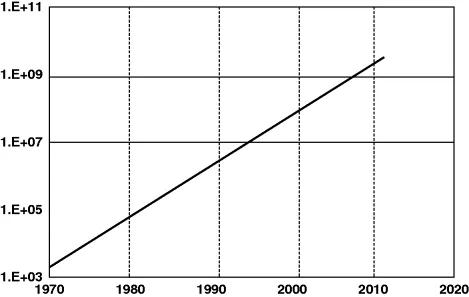
Much of the trend in the electronics industry has been driven by the concept of Moore's law [1], which says that the number of transistors on an integrated circuit chip doubles approximately every two years. This is illustrated in Figure 1.1, which shows the Intel CPU transistor count trend during the era of traditional metalāoxideāsilicon field-effect transistor (MOSFET) scaling [2]. Because the individual silicon wafer is the unit of measurement of production in the semiconductor industry, this law normally ends up meaning that the number of bits on a wafer must increase over time. This can occur by the wafer getting larger, the size of the chip shrinking, or the bit capacity increasing. Technology scaling and wafer-size increases result from engineering improvements in the technology. Chip capacity and performance increases are driven by the demands of the application. These application demands are driving the move to 3D vertical memories.
Figure 1.1 Illustration of Moore's law showing transistor count trend In Intel CPUs (Based on M. Bohr, IEDM, 2011 [2].)
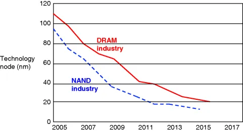
Scaling the dimensions of the circuitry on the chip is the method that has been used to shrink the size of the chip over the past 30 years or so. Scaling the dimensions has become increasingly expensive such that the required cost reduction is harder to obtain. Some memory cell technologies permit multiple bits to be stored in a unit cell area, which increases the capacity. Figure 1.2 illustrates the trend in scaling of the mainstream DRAM and NAND flash memories over the past 10 years [3].
Figure 1.2 Scaling trends of DRAM and NAND flash 2005ā2015. (Based on N. Chandrasekaran, (Micron), IEDM, December 2013 [3].)
Memory storage devices tend to be useful test chips as process drivers for the technology because memories are repetitive devices that require thousands or even millions of tiny, identical circuits to each work as designed. This permits low-level faults to be analyzed statistically with great accuracy. The trend to 3D has started with memory.
There are a finite number of types of memory devices that have been with us for the last 30ā40 years and are still the mainstream memories today. These are the static RAM, dynamic RAM, and nonvolatile memories. While innovative, emerging memories have always been around, none has as yet replaced these three as the mainstays of semiconductor data storage.
1.3 Early RAM 3D Memory
1.3.1 SRAM as the First 3D Memory
The static RAMs were the first integrated circuit (IC) memory device. Historically, their chief attributes have been their fast access time as well as their stability, low power consumption in standby mode, and compatibility wit...
Table of contents
Cover
Title Page
Copyright
Acknowledgments
Chapter 1: Basic Memory Device Trends Toward the Vertical
Chapter 2: 3D Memory Using Double-Gate, Folded, TFT, and Stacked Crystal Silicon
Chapter 3: Gate-All-Around (GAA) Nanowire for Vertical Memory
Chapter 4: Vertical NAND Flash
Chapter 5: 3D Cross-Point Array Memory
Chapter 6: 3D Stacking of RAMāProcessor Chips Using TSV