Since the first edition was published in 2008, Atomic Layer Deposition (ALD) has emerged as a powerful, and sometimes preferred, deposition technology. The new edition of this groundbreaking monograph is the first text to review the subject of ALD comprehensively from a practical perspective. It covers ALD's application to microelectronics (MEMS) and nanotechnology; many important new and emerging applications; thermal processes for ALD growth of nanometer thick films of semiconductors, oxides, metals and nitrides; and the formation of organic and hybrid materials.
Trusted by 375,005 students
Access to over 1.5 million titles for a fair monthly price.
Atomic Layer Deposition (ALD) is a more recent variation on the older technology referred to as Chemical Vapor Deposition (CVD) [1]. In CVD, which was originally developed in the 1920s, a mixture of gases flows over a heated substrate causing a thin solid film to grow on the surface. This heated surface has to be hot enough to allow the surface reaction to proceed rapidly, so that commercially acceptable deposition rates are achieved. In the ideal case, there will be no reaction between the reactant gases in the gas phase, in other words no homogeneous reactions, which would cause the formation of particulates. The gases approaching the heated surface will be heated by gas phase conduction and should not react until they impinge on the surface where they form a solid film of deposited material by a heterogenoeous reaction. If a homogenoeous reaction takes place, in the worst case one can have particles forming in the gas phase and ending up embedded in the growing thin film, clearly an unacceptable result.
The optimum choice of reactants for a CVD process is generally a mixture of the most reactive gases available. This allows film deposition at the highest rates, and at the lowest substrate temperatures. Unfortunately, this choice leads to a high probability of gas phase reactions, which as noted can compromise the deposited film quality. It is this dichotomy which has fueled much of the CVD research over the last thirty years.
The present book will be a review of CVD’s newer variant, ALD. In this technique, the presentation of the two reactants to the heated surface is separated into two steps. In step one, the substrate is exposed to the first reactant after which this reactant is pumped away. During this exposure a monolayer of the first reactant adsorbs to the substrate, and remains after the chamber is evacuated. Then a second reactant is introduced into the chamber, and it reacts with the monolayer of the first reactant. This then forms one layer (generally less than one complete monolayer) of the solid film being sought. After this, the remaining second reactant and any gas phase reaction products are removed from the chamber. This process is repeated as many times as necessary to grow a film of the desired thickness. The conformality of the film is also excellent, since film growth depends only on the formation of monolayers on the surface and not on the arrival rate of reactants. The time necessary to form such a layer can be increased if necessary for a complex-shaped substrate and the arrival of excess reactant is not important. Clearly with this process, gas phase reactions should not occur, so that one is free to choose the most reactive reactants available and film deposition temperatures can be lower. However, the one disadvantage is that the film deposition rate may be slow. For those applications where thin, uniform and highly conformal films are of interest, this becomes less of a limitation and ALD is an important process.
To set the scene for a description of ALD, the characteristics of the CVD process will be described.
1.1.1 Thermal CVD
The first CVD processes that had major commercial importance were developed when researchers were required to find ways to deposit thin films of dielectrics and semiconductors on semiconductor wafers. These initial processes were all mostly carried out by simply heating a substrate and placing it in a gas stream of one or more reactants. Initially all the processes were run at atmospheric pressure.
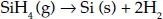
One of the first thin films to be deposited was silicon, because in the early days single crystal wafers were not pure enough to allow integrated circuits to be built into them directly. The CVD silicon films, on the other hand, could be grown at very high purity from carefully purified reactant gases. Among the reaction schemes used were
(1.1)
(1.2)
(1.3)
(1.4)
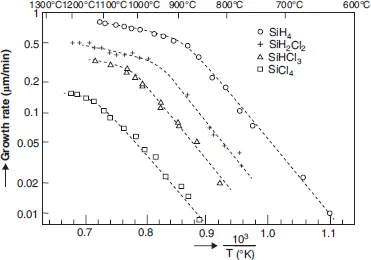
Any of these four reactions can be used to deposit silicon, and the film morphology can be single crystal, polycrystalline or amorphous, depending on the deposition temperature. A typical plot of deposition rate versus deposition temperature for these four reactions is shown in Figure 1.1 below.
Figure 1.1 Silicon growth rate as a function of temperature [2].
As can be seen, the lowest growth rates at a given temperature are for the silicon tetrachloride reaction (Eq. 1.2), because this molecule is the most stable of the four silicon precursors. The highest growth rates are seen for the silane reaction (Eq. 1), as this molecule is the least stable of the four. At the higher temperatures, to the left in the Figure, single crystal (epitaxial films) can be grown. At the lower temperatures, to the right, one obtains either amorphous or polycrystalline films.
Generally, the silicon tetrachloride reaction has been commercially preferred, in spite of the high temperatures needed. Partly, this is because this reaction involves molecules that are likely to remain stable as the gas approaches the hot wafer surface, and gas phase reactions are less likely. At the other extreme we have the silane reaction, where this molecule is not a very stable species. Although deposition can be carried out at lower temperatures, there is the risk of gas phase nucleation leading to lower quality epitaxial films.
We also have to note the shape of these curves. When commercially desirable deposition rates are demanded, then deposition at high temperatures is necessary, and we see that the deposition rate is relatively independent of temperature. This is referred to as the diffusion limited regime of CVD. Here, the deposition rate is controlled by the arrival rate of reactant species which diffuse to the surface from the gas stream. The difficulty here is that the film uniformity over large areas depends very much on fluid flow uniformity. Particularly for reactors that coat several substrates at one time, such flow uniformity can be hard to achieve.
If depositions are carried out at lower temperatures, we see that deposition rates vary almost linearly on this semilog plot., that is the deposition rate reduces exponentially with the reciprocal of the temperature. Also we see that deposition rates become very low, and in order for a reactor to be commercially viable one must process many wafers at one time. Now, the deposited film uniformity depends strongly on temperature so it is mandatory that the batch reactor have a very uniform temperature.
Aside from semiconductors such as silicon, many commercially important materials can be deposited as thin films by CVD, such as metals (e.g. tungsten, copper), refractory metal silicides (e.g. tungsten silicide), nitrides (e.g. titanium nitride, silicon nitride), and of course oxides (e.g. silicon dioxide). In addition, CVD is an important process for deposition in non-semiconductor applications such as wear-resistant coating for tools [3] and catalysts [4] and recently for the deposition of carbon nanotubes [5], graphene layers [6], polymers [7] and many other materials.
In summary then, thermal CVD has been a powerful process for the commercial deposition of high quality thin films of many different materials. The process, however, has only proven useful with a restricted range of precursors because of the conflict between the use of the most reactive species in order to obtain the highest deposition rate at low temperature, which may lead to homogeneous reactions and poorer film properties, and the very high temperatures required when less reactive species are chosen but which may give better film properties. One way out of this dilemma is to use a less reactive precursor, but enhance its reactivity by creating a glow discharge in the flowing gases. This topic will be reviewed in the next section.
1.1.2 Plasma Enhanced CVD (PECVD)
Thermal CVD is a process that, although occurring in a flowing chemically reacting gas which is inherently not in thermodynamic equilibrium, occurs close to equilibrium. On the other hand, when a glow discharge is created in a gas at low pressure the resulting plasma is very far from thermal and chemical equilibrium. That is, the electrons in the plasma tend to be very energetic and the ions and molecular species tend to have low energies. For typical situations the electrons can have energies consistent with temperatures of many thousands of degrees, and as a result readily dissociate a substantial number of the molecular species in the reacting gas mixture.
Historically, glow discharges in reacting gas mixtures have been used to lower the required deposition temperatures below those required by thermal processes. This allowed deposition at practical deposition rates of a number of commercially important films. For example, silicon nitride deposited at over 800°C could not be used to passivate an integrated circuit, because aluminum conducting layers would have melted. When silane and ammonia mixtures were used in a low pressure glow discharge, deposition at acceptable rates could be achieved at much lower temperatures ~ 350°C. Accordingly, PECVD of silicon nitride became a standard final passivation layer, and integrated circuits could be reliably packaged in low cost plastic. Prior to this all circuits had to be hermetically sealed in ceramic packages.
There are a number of issues to consider when plasma is used to activate a CVD reaction. The plasma can provide the energy for the chemical reaction and it can create reactive radicals which react more easily than the precursor molecules. However, it can also contain ions and hot electrons which can impinge on the substrate and can have both helpful and deleterious effects on the deposited film and the substrate surface. Bombardment by ions can cause stress, typically compressive stress, which can densify the film and reduce the likelihood of cracking. The ion bombardment can a...
Table of contents
Cover
Half Title page
Title page
Copyright page
Acknowledgements
Foreword
Preface
Chapter 1: Fundamentals of Atomic Layer Deposition
Chapter 2: Elemental Semiconductor Epitaxial Films
Chapter 3: III-V Semiconductor Films
Chapter 4: Oxide films
Chapter 5: Nitrides and Other Compounds
Chapter 6: Metals
Chapter 7: Organic and Hybrid Materials
Chapter 8: ALD Applications and Industry
Index
Frequently asked questions
Yes, you can cancel anytime from the Subscription tab in your account settings on the Perlego website. Your subscription will stay active until the end of your current billing period. Learn how to cancel your subscription
No, books cannot be downloaded as external files, such as PDFs, for use outside of Perlego. However, you can download books within the Perlego app for offline reading on mobile or tablet. Learn how to download books offline
Perlego offers two plans: Essential and Complete
Essential is ideal for learners and professionals who enjoy exploring a wide range of subjects. Access the Essential Library with 800,000+ trusted titles and best-sellers across business, personal growth, and the humanities. Includes unlimited reading time and Standard Read Aloud voice.
Complete: Perfect for advanced learners and researchers needing full, unrestricted access. Unlock 1.5M+ books across hundreds of subjects, including academic and specialized titles. The Complete Plan also includes advanced features like Premium Read Aloud and Research Assistant.
Both plans are available with monthly, semester, or annual billing cycles.
We are an online textbook subscription service, where you can get access to an entire online library for less than the price of a single book per month. With over 1.5 million books across 990+ topics, we’ve got you covered! Learn about our mission
Look out for the read-aloud symbol on your next book to see if you can listen to it. The read-aloud tool reads text aloud for you, highlighting the text as it is being read. You can pause it, speed it up and slow it down. Learn more about Read Aloud
Yes! You can use the Perlego app on both iOS and Android devices to read anytime, anywhere — even offline. Perfect for commutes or when you’re on the go. Please note we cannot support devices running on iOS 13 and Android 7 or earlier. Learn more about using the app
Yes, you can access Atomic Layer Deposition by Tommi Kääriäinen,David Cameron,Marja-Leena Kääriäinen,Arthur Sherman in PDF and/or ePUB format, as well as other popular books in Technology & Engineering & Materials Science. We have over 1.5 million books available in our catalogue for you to explore.