![]()
Chapter 1
Overview of Atomic Force Microscopy
Dalia G. Yablon
SurfaceChar LLC, Sharon, MA
Atomic force microscopy (AFM) is a family of nanoscale characterization techniques that has exploded onto the overall characterization and nanotechnology field as its versatility and high resolution continue to feed a dizzying variety of disciplines from biology to physics and chemistry to engineering. AFM entered the scientific arena in 1981 with the now famous invention of its older sibling in the scanning probe microscopy family, the scanning tunneling microscope (STM) in the IBM Zurich labs of Gerd Binnig and Heinrich Rohrer, for which they received the Nobel Prize in Physics in 1986. The AFM was then invented in 1986 by Gerd Binnig, Cal Quate, and Christoph Gerber [1]. Together, STM and AFM formed the scanning probe microscopy (SPM) family, which includes other methods such as near-field scanning optical microscopy (NSOM).
The STM spawned the next 25 years of the continuously developing field of scanning probe microscopy and specifically atomic force microscopy, which now includes dozens of different methods under its name to probe various properties—including mechanical, electrical, magnetic, chemical, and optical—of materials and surfaces. Atomic force microscopy is a powerful tool in various research enterprises. It is found in practically any university characterization facility alongside optical and electron microscopes, and most undergraduates in science or engineering fields at this point are at least familiar with it, if not have performed a laboratory experiment in their undergraduate curriculum.
The focus of this book is to understand and appreciate the role this young technique has played in industrial research and development (R&D). AFM has penetrated into a variety of industrial research sectors as witnessed by the diverse set of applications described in this book. Alongside electron and optical microscopy, which have been around for decades and have reached an impressive level of commercial maturity and ease of use, AFM has become a vital characterization method despite its youth and continued technical evolution. So, though AFM is still an active area of academic research as its capabilities continue to develop and be better understood, it has proven to be a useful microscopy to address industrial and commercial needs from quality control and assurance to product formulation and process monitoring.
The goal of this introductory chapter is to provide an overview of AFM to nonspecialists and introduce the various topics that are the subject of subsequent individual chapters. As such, this chapter will provide a brief review of the beginnings of AFM and special features that make it particularly suited for industrial research. Then a brief overview of AFM operation will be presented including the hardware, software, calibrations involved, and finally the different nanomechanical methods that will be described in detail both in theory and application. Entire books are written on AFM operation, and this chapter is not meant to be an exhaustive introduction to its operation, merely serving to provide enough information for the rest of the book to be followed intelligently. Readers interested in more detail about AFM operation can consult a number of excellent books on the topic [2–5].
1.1 A WORD ON NOMENCLATURE
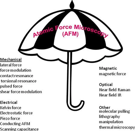
Before the rest of this chapter continues, some definitions are in order. Similar to many other surface science techniques, AFM has succumbed to a somewhat unwieldy mess of abbreviations and jargon that has become a hard-to-navigate alphabet soup. SPM refers to an umbrella of a variety of methods. Methods that fall under SPM include perhaps its most famous member, atomic force microscopy (AFM), in addition to others such as scanning tunneling microscopy (STM), near-field scanning optical microscopy (NSOM or SNOM, depending on the continent), and other lithographic methods. And then within AFM there are dozens of methods that rely on the AFM probe–sample interactions to provide a variety of material properties including electrical, optical, magnetic, and mechanical properties. To date, there are dozens of SPM/AFM-based methods. It is beyond the scope of this book to list and/or define all the related methods. These methods characterize a huge variety of material properties. Some of the more common methods have been included in Figure 1.1 with the category of properties that they measure. The wide diversity of properties of materials that can be measured with AFM is clear. The focus of this book is on nanomechanical characterization, due to its broad appeal in industrial R&D. Again, Figure 1.1 is offered to demonstrate the variety and flavor of properties that can be probed with SPM.
1.2 ATOMIC FORCE MICROSCOPY—THE APPEAL TO INDUSTRIAL R&D
This book specifically focuses on AFM, which is the method that has most penetrated the general characterization and industrial research fields. AFM has key features that make it especially attractive to industrial research and development. First, its resolution, the heart of its utility as a characterization tool, is indeed impressive with 5- to 10-nm lateral resolution and angstrom vertical resolution achieved routinely on commercial instruments with commercial cantilevers. The limits of lateral resolution continues to be pushed with specialized techniques and cantilevers, and it has reached true “atomic” resolution where point defects of certain materials can now be imaged under certain operating parameters and imaging modes, especially under liquid [6–8]. True atomic resolution is still currently mostly achieved through STM, which operates through an entirely different tip–sample interaction mechanism based on quantum mechanical tunneling. Many of these STM studies are conducted in ultrahigh vacuum (UHV), though some are performed in ambient and liquid conditions. It is fair to say that AFM is catching up, however, with recent groundbreaking work imaging cyclic aromatic molecules on Cu[111] [10, 11].
A second critical feature of AFM that makes it particularly amenable to industrial research is the flexibility of the environment in which it can operate. Despite being a high-resolution microscopy that rivals the resolution of electron microscopy, AFM can operate in an ambient or even liquid environment with minimal compromise to its resolution. The ability to work in “real-world” environments makes it a critical tool for many industrial R&D applications, where the research emphasis is consistently to understand mechanisms and materials in real-world situations as opposed to idealized materials and conditions that typically exist in academic research endeavors. In many cases, the researcher may not want the sample to be forced into a pristine vacuum environment where perhaps key materials or components will be evacuated and thus missed in the characterization effort. In addition, the flexibility of an environment permits in situ characterization of processes. For example, processes such as corrosion, lubrication, catalyst dissolution, crystal growth (for active pharmaceutical ingredient, API) can all be studied in situ with AFM as a unique attribute of this microscopy. The power of in situ measurements for biological applications is simple as many biological processes and materials simple cannot survive ex situ.
A corollary of the utility of the AFM’s flexible environment to industrial R&D is the flexibility of type and shape of surface or material that AFM can image. There are virtually no restrictions on the size of a material that can be probed with AFM. Many commercial “large-sample” AFMs currently exist that can image any design or shape of a surface from engine parts to thin films. Indeed, one of the AFMs built in the early 1990s (Topometrix Explorer) was advertised as being able to be placed on top of jet wings to image fractures. In addition, there are practically no mechanical or electrical restrictions on the type of sample an AFM can image. Unlike electron microscopy or STM that require conducting or semiconducting surfaces to image or avoid artifacts [or in the case of insulating surface in scanning electron microscopy (SEM) that requires deposition of a thin conducting layer such as Cr], AFM can image insulating surfaces in addition to conducting or semiconducting surfaces with minimal sample prep. Typically, the most significant requirement on the sample for an AFM is that it be smooth. Commercial instruments will have a maximum z (vertical) range that can be imaged, dictated by the design and desired resolution of the particular instrument. The maximum z range is typically from 1 µm (for high-resolution studies) to several microns (for lower resolution studies), meaning that the sample cannot have features, a tilt, or overall roughness that exceed that limit in order for the AFM to image effectively. Smooth surfaces are often prepared with the use of an ultramicrotome. An ultramicrotome is simply a very controlled and precise way of cutting of thin (down to 100 nm) sections, at controlled speeds and in a controlled fashion to result in ultrasmooth surfaces of nanometer or less than nanometer roughenss. The ultramicrotome typically employs the use of a glass knife for a coarse cut and then a diamond knife for a fine cut. Cryomicrotomy is simply ultramicrotomy at cold temperatures. Cryomicrotomy is typically used to prepare polymer surfaces to cut below the glass transition temperature of the material; depending on the instrument, cryomicrotomes can cool down to -180°C.
Finally, AFM is fundamentally a mechanical probe of the surface through actual contact between the tip and sample. So, in addition to the ability to provide high resolution on surface features, the goal of any form of microscopy is the unique tip–sample interaction mechanism enabling the probing of many properties, most obvious of which is mechanical properties. Mechanical properties covers a wide range of materials and properties. Entire textbooks and courses are devoted to the studies of mechanics, for example, by Callister and Rethwisch [12]. We very briefly review some of the main concepts below to provide enough of a background for the rest of the chapter.
This edition focuses specifically on nanomechanical characterization. Probing other material properties such as optical, electrical, or magnetic properties is not covered in this book. The reason is that though these other properties have been successfully probed in various industrial R&D applications, using AFM to probe mechanical properties of surfaces is more ubiquitous in industrial R&D, and so was a logical focus for a first book on SPM in industrial...