![]()
Chapter 1
Introduction to the Theory and Advantages of Low Voltage Electron Microscopy
David C. Bell1 and Natasha Erdman2
1School of Engineering and Applied Sciences, Harvard University, USA
2JEOL USA Inc., USA
1.1 Introduction
The fundamental aspects of electron microscopy all relate directly to the physics of the interactions between the electron beam and sample. These interactions have been studied extensively since the discovery of the electron by J.J. Thompson in 1897. Energetic electrons are described as “ionizing radiation”—the general term used to describe radiation that is able to ionize or remove the tightly bound inner shell electrons from a material. This is obviously an advantage for electron microscopy in that it produces a wide range of secondary signals such as secondary electrons and X-rays, but is also a disadvantage from the perspective that the sample is “ionized” by the electron beam and possibly structurally damaged, which depending on the accelerating voltage happens in a number of different ways. The advantages of using a lower accelerating voltage for the electron beam are that the energy is reduced and hence the momentum that can be transferred to sample from the electron is also reduced. This, however, has the unwanted effect of reducing the possible emitted signal; although, with recent improvements in detectors, cameras and the use of aberration correctors, the signal to noise and the resolution to produce a final image can not only be maintained but are actually improved.
This chapter will detail the basic theory of electron beam interactions and how it relates to electron microscopy at low voltage. There are, however, distinct differences between the important considerations for low voltage SEM imaging as compared to TEM imaging and these will be detailed in the text.
1.2 Historical Perspective
The early steps in the development of the electron microscope in the 1930s and 1940s by different research groups led ultimately to the development of two distinct groups of instruments: the scanning electron microscope (SEM) and the transmission (or scanning transmission) electron microscope (TEM and STEM). The early microscope designs by Knoll and by Ruska (1933) showed transmission electron images of solid surfaces at 10–16X magnification, which was improved upon by introduction of replica sample preparation technique for TEM observation (Mahl, 1940). As a continuation of his work with Ruska, M. Knoll had designed an electron beam scanner in 1935 (Knoll, 1935) to study targets for the TV camera tubes; this was in essence a predecessor to an SEM, with accelerating voltage up to 4 kV. In 1936 through his contract with the company Siemens, Manfred von Ardenne began development of a scanning transmission electron microscope, mainly to avoid detrimental effects of chromatic aberration during observation of thick specimens in TEM. The microscope built by von Ardenne had a probe size of 4 nm (von Ardenne, 1937; von Ardenne 1938). The work by von Ardenne, though interrupted by the events of World War II, nonetheless established a theoretical and design background for future SEM and STEM development, particularly regarding understanding of beam/specimen interactions, effect of accelerating voltage on resolution, as well as detector design and positioning within the microscope (von Ardenne, 1985).
From 1938 to 1942, V. Zworykin at RCA headed parallel SEM and TEM development projects that resulted in an SEM instrument with accelerating voltage of 800V (Zworykin et al., 1942). However, poor vacuum in the system significantly impacted the resulting micrographs, and the quality of the recorded images was disappointing with mostly topographic contrast and no meaningful compositional information. These results prompted RCA to discontinue the SEM project and concentrate on the development of the TEM instrument, and led to the development of several commercial instruments. Nonetheless, the work on SEM instrument development continued in Cambridge in early 1950s (McMullan, 1952; McMullan, 2004). R.F.M. Thornley successfully developed the first low voltage SEM (Thornley, 1960) in Oatley's lab at Cambridge University in the early 1960s. By improving upon the existing SEM2 design (Wells, 1957), he was able to obtain 200 nm probe at 1 kV. Prior to that experiment, the SEM was always operated at higher voltages (greater than 6 kV) that allowed only observation of conductive specimens. Thornley's work showed that a surface of alumina ceramic could be imaged at 1.5 kV negating charging artifacts (Thornley, 1960); moreover, he recognized the importance of low voltage in reducing the charge build up that had caused issues in non-conductive samples.
Over the years, significant improvements in electronics, vacuum and electron column design, as well as detector technology have improved SEM instrument performance to the level where the resolution at 1 kV is on the order of 1–2 nm for high-end field emission systems (see Chapter 2). The recent developments in aberration correction and addition of monochromators to TEM and STEM instruments have further improved their performance for both high and low accelerating voltage applications (see Chapters 6–8).
1.3 Beam Interaction with Specimen—Elastic and Inelastic Scattering
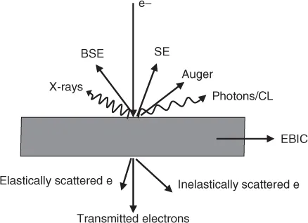
Interaction of a primary electron beam with specimen can generate several different signals (Figure 1.1)—secondary and backscatter electrons, transmitted electrons (if the specimen is sufficiently thin), Auger electrons, characteristic X-rays and photons.
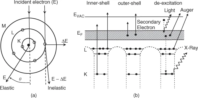
The basic elastic and inelastic scattering processes and electron excitation in materials have a direct influence on the electron range and depth of ionization distribution as well as secondary and backscatter electron emission and the observed contrast in all types of electron microscopes. Particle model of elastic and inelastic scattering processes (based on Bohr atom model) is shown in Figure 1.2(a), while Figure 1.2(b) displays band structure with inelastic processes as well as Auger and X-ray emissions, with respect to different energy levels. Multiple elastic scattering events produce electron backscattering; additional multiple inelastic scattering processes lead to eventual energy loss along the electron trajectories deeper within the material that result in the electrons slowing down and eventually coming to rest. Inelastic scattering is also responsible for the generation of secondary electron signal, Auger electrons, X-rays, electron–hole pairs (semiconductors and insulators), cathodoluminescence and phonon and plasmon production. At lower accelerating voltages, the number of inelastic scattering events decreases; for example, in Si K-shell ionization is no longer possible if accelerating voltage is below 1.84 kV, an effect known as the Duane-Hunt limit.
Understanding of the elastic and inelastic scattering processes can additionally serve as a basis for modeling of beam/specimen interactions (particularly for SEM imaging and analysis) via Monte–Carlo simulations to investigate electron trajectories in materials and calculate theoretical secondary and backscatter electron spatial distributions based on the specimen position under the beam (angle), accelerating voltage and the material type. Several different programs are available for these types of calculations; more specifically Casino (Drouin et al., 2007; also http://www.gel.usherbrooke.ca/casino/index.html) has been written particularly with a focus on low voltage imaging and analysis.
The quantum mechanical properties of electron are such that the electron has a wavelength defined by de Broglie relationship:
1...