eBook - ePub
Nonvolatile Memory Technologies with Emphasis on Flash
A Comprehensive Guide to Understanding and Using Flash Memory Devices
- English
- ePUB (mobile friendly)
- Available on iOS & Android
eBook - ePub
Nonvolatile Memory Technologies with Emphasis on Flash
A Comprehensive Guide to Understanding and Using Flash Memory Devices
About this book
Presented here is an all-inclusive treatment of Flash technology, including Flash memory chips, Flash embedded in logic, binary cell Flash, and multilevel cell Flash. The book begins with a tutorial of elementary concepts to orient readers who are less familiar with the subject. Next, it covers all aspects and variations of Flash technology at a mature engineering level: basic device structures, principles of operation, related process technologies, circuit design, overall design tradeoffs, device testing, reliability, and applications.
Trusted by 375,005 students
Access to over 1.5 million titles for a fair monthly price.
Study more efficiently using our study tools.
Information
1
INTRODUCTION TO NONVOLATILE MEMORY
1.1 INTRODUCTION
In this introductory chapter the ABCs of nonvolatile memory are reviewed. The purpose of this elementary discussion is to provide the perspective necessary for understanding the much more detailed chapters that follow. The emphasis is on communication of an overview, rather than on specifics of implementation. Simple memory concepts and terminology are presented, the parameters and features unique to nonvolatile memory (NVM for short) are examined, generic Flash memory variants are described, and finally the treatment of NVM in the International Technology Roadmap for Semiconductors (ITRS) is described.
Semiconductor memory is an essential part of modern information processors, and like all silicon technology it has been more or less growing in density and performance in accordance with Moore’s law. Semiconductor NVM technology is a major subset of solid-state memory. Nonvolatility, of course, means that the contents of the memory are retained when power is removed. This book provides an in-depth description of semiconductor-based nonvolatile memory including basic physics, design, manufacture, reliability, and application. Flash memory is emphasized because for a long period of time it has been the dominate form of NVM both in terms of production volume and magnitude of sales dollars. Flash, however, is not the only alternative, and this book also attempts to describe some of the many NVM technologies that have some hope of achieving success in the marketplace.
1.2 ELEMENTARY MEMORY CONCEPTS
All information processing can be viewed as consisting of the sequential actions of sensing, interpreting/processing, and acting. These actions cannot be accomplished without somehow remembering the item of interest at least long enough to allow the operations to take place, and most likely much longer to allow convenient use of the raw data and/or the end results.
The length of time that the memory can retain the data is the property called retention, and the unpowered retention time parameter is the measure of nonvolatility. A volatile memory will typically have a worst-case retention time of less than a second. A nonvolatile memory is usually specified as meeting a worst-case unpowered retention time of 10 years, but this parameter can vary from days to years depending on the specific memory technology and application.
Integrated circuit nonvolatile memories are frequently classified in terms of the degree of functional flexibility available for modification of stored contents. Table 1.1 summarizes the categories currently in frequent use [1]. This class of memory was evolved from ultraviolet (UV) erasable read-only memory (ROM) devices, and thus the category labels contain “ROM” as a somewhat awkward reminder of that heritage.
Flash memory [2] is an EEPROM where the entire chip or a subarray within the chip may be erased at one time. There are many variants of Flash, but present-day production is dominated by two types: NAND Flash, which is oriented toward data-block storage applications, and common ground NOR Flash, which is suited for code and word addressable data storage.
In general, information processing requires memory, but it is not at all clear that any constraints are placed on the structure or location of the storage relative to the processing elements. That is, the memory may be a separate entity and entirely different technology than the logic, or it may be that the logic is embedded in the memory and be a technology compatible with the logic, or any combination thereof.
At the heart of every memory is some measurable attribute that can assume at least two relatively stable states. Many common memory devices are charge based where charge can be injected into or removed from a critical region of a device, and the presence or absence of the charge can be sensed. The process of setting the charge level is called writing, and the process of sensing the charge level is called reading. Alternatively, the write operation may be referred to as the store operation, and the read operation may be called the recall operation.
TABLE 1.1. Nonvolatile Memory Functional Capability Classifications
| Acronym | Definition | Description |
| ROM | Read-only memory | Memory contents defined during manufacture and not modifiable. |
| EPROM | Erasable programmable ROM | Memory is erased by exposure to UV light and programmed electrically. |
| EEPROM | Electrically erasable programmable ROM | Memory can be both erased and programmed electrically. The use of “EE” implies block erasure rather than byte erasable. |
| E2PROM | Electrically erasable programmable ROM | Memory can be both erased and programmed electrically as for EEPROM, but the use of “E2” implies byte alterability rather than block erasable. |
Dynamic random-access memory (DRAM), a volatile technology, uses charge stored on a capacitor to represent information. Charge levels greater than a certain threshold amount can represent a logic ONE, and charge levels less than another threshold amount can represent a logic ZERO. The two critical levels are chosen to assure unambiguous interpretation of a ZERO or ONE in the presence of normal noise levels. (Here the higher charge level has been called a ONE, but it is arbitrary which level is defined to be the ONE or ZERO.)
Leakage currents and various disturb effects limit the length of time that the capacitor can hold charge, and thus limits “powered” retention to short periods. The word “dynamic” in the name “DRAM” indicates this lack of ability to hold data continuously even while the circuit is connected to power. Each time the data is read, it must be rewritten in order to assure retention, and regular data refresh operations must be performed when the cell is idle. Worst-case retention time (i.e., the shortest retention time for any cell within the chip) is typically specified as about 60 ms. DRAM is a volatile memory in terms of “unpowered” retention because the charge is not maintained when the circuit power supply is turned off.
Flash memory makes use of charge stored on a floating gate to accomplish nonvolatile data storage. Figure 1.1 provides a cartoon cross-section sketch of a floating-gate transistor and its circuit symbol representation. The floating-gate electrode usually consists of a polysilicon layer formed within the gate insulator of a field-effect transistor between the normal gate electrode (the control gate) and the channel. The amount of charge on the floating gate will determine whether the transistor will conduct when a fixed set of “read” bias conditions are applied. The fact that the floating gate is completely surrounded by insulators allows it to retain charge for a long period of time independent of whether the circuit power supply voltage is present. The act of reading the data can be performed without loss of the information.
Figure 1.2 compares an imaginary idealized transistor with no charge layer in the gate insulator with a transistor that has a charge per unit area, Q, at distance d from the silicon channel surface. The impact of the charge on the threshold voltage depends on the amount of charge per unit area, its distance from the silicon surface, and the permittivity of the insulator between the charge and the silicon. In a Flash device the floating gate provides a convenient site for the charge, but other means may serve the same purpose. For example, in silicon oxide nitride oxide silicon (SONOS) transistors the charge will reside in traps within the nitride layer.
Figure 1.1. Floating-gate transistor: (a) elements of the transistor structure and (b) circuit symbol.
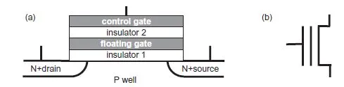
Figure 1.2. VTH shift due to charge in gate insulator.
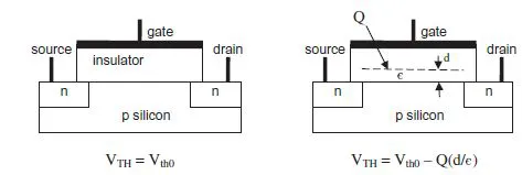
Figure 1.3. Shift of current–voltage characteristics because of inserted charge.
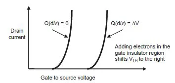
The threshold voltage, of course, impacts how the source-to-drain current of the transistor will change as a function of change in the gate-to-source voltage. Figure 1.3 shows how the characteristic curves can be made to shift as a function of the stored charge. As electrons are added to the charge within the gate insulator region, the curve will move in a positive direction.
For some memory technologies the process of reading destroys the data. This is referred to as destructive readout (DRO). For other technologies, Flash, for example, readout can be accomplished without significantly disturbing the data. This is referred to as nondestructive readout (NDRO). DRO memory has the disadvantage of requiring that every read operation must be followed by a write operation to restore the data.
Over time some forms of memory organization have been so firmly established that most engineers immediately assume those structures and the parameters that characterize those structures as being the norm. Probably the most pervasive assumption is that the information to be stored and recalled is in a digital binary format.
There are several schemes where a single transistor may be used to store more than just one bit. One approach is to store charge in physically separated parts of the device that can be sensed separately. Currently, the most common example of this concept is the NROM cell discussed later in this chapter. Another approach is to interpret the amount of charge stored in one physical location in the device as a representation of a multibit binary number. In this case the sensing process must reliably distinguish between different quantities of stored charge and the readout process must generate the corresponding binary number.
Consider the “one physical location” approach. A 1-bit-per-cell arrangement is a robust form of storage that allows relaxed margins and comparatively simple sensing circuitry. The read current needs only to be unambiguously above or below a preset value in order to establish whether a ONE or a ZERO was stored. For a 2-bit-per-cell memory, the recall process must reliably distinguish between four preset levels of charge, and the readout circuitry must translate the detected level into a 2-bit digital format. The storage process and the protection of the cell from disturb conditions must accurately set and maintain those four levels under all operating and nonoperating storage conditions. Considering that the usual requirement is for nonvolatile data retention for 10 years, assuring stability of charge levels and circuit characteristics is quite a challenge. Of course, the complexity rapidly increases as a cell is required to store larger numbers of bits. For example, a 4-bit-per-cell memory must reliably cope with 16 levels and still meet all specifications.
While the heart of a semiconductor memory is the cell, the surrounding circuitry is the mechanism that makes it usable. For economic reasons, cells are packed as close together in a rectangular planar array as available integrated circuit technology and noise management concerns will allow. This X,Y array arrangement contains the cells and conductive lines that allow access to each individual cell.
The lines that run in the X direction (rows) are called wordlines, and they are used to select a row of cells during the write or read operations. Wordlines tie to the control gates of the cells in a row. The lines that run in the Y direction (columns) are called bitlines. As shown in Figure 1.4, bitline connections for the NOR array architecture are tied to drain terminals of devices in a column. One end of a bitline connects to power and then goes through the array to sensing and writing circuitry. Thus the wordlines activate a specific group of cells in a row, and the bitlines for each intersecting column connect those cells to read and write circuits.
In the example of a NOR architecture, the cells in a column are connected in parallel where all the drain terminals tie to a bitline and all the source terminals tie to a common source line (ground). In this configuration a positive read mode voltage on one wordline while all other wordlines are at zero volts will result in a bitline current that is a function only of the selected row of cells.
This, of course, assumes that a zero control gate-to-source voltage actually turns off the unselected rows. For the NOR organization it is important that the process of initializing the array, called erase, not proceed to the point of overerasing transistors to the extent that the threshold voltage becomes negative and the transistors change from operation in the enhancement mode to operation in the depletion mode.
The NAND array architecture, shown in Figure 1.5, achieves higher packing density. Here the bitlines are formed using series-connected strings of cells that do not require contact holes. A string is typically 8, 16, or 32 cells long. If other strings were to be tied to the same bitlines, they would be connected in parallel between the bitline and the common source line in a manner similar to individual cells in the NOR architecture.
Figure 1.4. NOR array architecture.
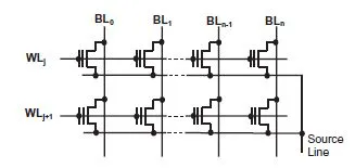
Figure 1.5. NAND array architecture.
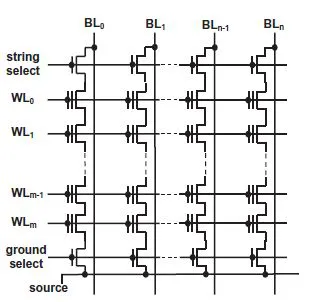
Reading and writing a NAND device is more complicated than dealing with a NOR device. The wordlines are used to select the transistor of interest in the string. To access data from a string, the reading process requires that all nonselected transistors be turned on while only the selected transistor is allowed to influence the current flow through the string. In contrast to the NOR architecture, it is not objectionable to allow the transistors to be shifted into depletion mode. There are, however, problems if transistors are shifted too far in the enhancement direction. It is important that the distribution of threshold voltages for the programmed state be limited to a specified design range in order to assure proper circuit operation.
There are a number of basic principles of operation that apply to both NOR and NAND organized devices. For a single read operation the individual bits that form a word are made to appear in an input/output register. For a single write operation the word present in an input/output register is used to determine the data inserted into the cells for that word. Reading or writing processes must be designed such that unselected cells are not disturbed while the selected cells are operated on. The design of the array must contend with basic circuit design issues associated with driving heavily loaded transmission lines as well as assuring proper operation of each individual cell.
In order to select a given row and column an integrated memory device is usually provided with a binary address word from external circuitry. The address word is routed to address decoder circuitry that is tightly tied to the sides of the array, and designed to drive the word and bitlines. For reasons of management of loading and data grouping considerations, large memory chips are usually partitioned into many arrays.
A modern integrated memory device incorporates control circuitry that accepts relatively simple commands as inputs and generates timed sequences of signals to accomplish writing, reading, and various other modes of operation. Also, the writing operations may require voltages that differ from the readily available normal logic supply voltages. In order to simplify the use of the device these voltages are typically generated on-chip. This feature also has the advantage of allowing the semiconductor manufacturer t...
Table of contents
- Cover
- Series
- Title
- Copyright
- Foreword
- Preface
- Contributors
- 1: INTRODUCTION TO NONVOLATILE MEMORY
- 2: FLASH MEMORY APPLICATIONS
- 3: MEMORY CIRCUIT TECHNOLOGIES
- 4: PHYSICS OF FLASH MEMORIES
- 5: NOR FLASH STACKED AND SPLIT-GATE MEMORY TECHNOLOGY
- 6: NAND FLASH MEMORY TECHNOLOGY
- 7: DINOR FLASH MEMORY TECHNOLOGY
- 8: P-CHANNEL FLASH MEMORY TECHNOLOGY
- 9: EMBEDDED FLASH MEMORY
- 10: TUNNEL DIELECTRICS FOR SCALED FLASH MEMORY CELLS
- 11: FLASH MEMORY RELIABILITY
- 12: MULTILEVEL CELL DIGITAL MEMORIES
- 13: ALTERNATIVE MEMORY TECHNOLOGIES
- Index
- About the Editors
Frequently asked questions
Yes, you can cancel anytime from the Subscription tab in your account settings on the Perlego website. Your subscription will stay active until the end of your current billing period. Learn how to cancel your subscription
No, books cannot be downloaded as external files, such as PDFs, for use outside of Perlego. However, you can download books within the Perlego app for offline reading on mobile or tablet. Learn how to download books offline
Perlego offers two plans: Essential and Complete
- Essential is ideal for learners and professionals who enjoy exploring a wide range of subjects. Access the Essential Library with 800,000+ trusted titles and best-sellers across business, personal growth, and the humanities. Includes unlimited reading time and Standard Read Aloud voice.
- Complete: Perfect for advanced learners and researchers needing full, unrestricted access. Unlock 1.5M+ books across hundreds of subjects, including academic and specialized titles. The Complete Plan also includes advanced features like Premium Read Aloud and Research Assistant.
We are an online textbook subscription service, where you can get access to an entire online library for less than the price of a single book per month. With over 1.5 million books across 990+ topics, we’ve got you covered! Learn about our mission
Look out for the read-aloud symbol on your next book to see if you can listen to it. The read-aloud tool reads text aloud for you, highlighting the text as it is being read. You can pause it, speed it up and slow it down. Learn more about Read Aloud
Yes! You can use the Perlego app on both iOS and Android devices to read anytime, anywhere — even offline. Perfect for commutes or when you’re on the go.
Please note we cannot support devices running on iOS 13 and Android 7 or earlier. Learn more about using the app
Please note we cannot support devices running on iOS 13 and Android 7 or earlier. Learn more about using the app
Yes, you can access Nonvolatile Memory Technologies with Emphasis on Flash by Joe Brewer, Manzur Gill, Joe Brewer,Manzur Gill in PDF and/or ePUB format, as well as other popular books in Technology & Engineering & Electrical Engineering & Telecommunications. We have over 1.5 million books available in our catalogue for you to explore.