![]()
PART 1
FUNDAMENTALS
![]()
Chapter 1
Surface and Colloidal Chemical Aspects of Wet Cleaning
Srini Raghavan, Manish Keswani, and Nandini Venkataraman
Department of Materials Science & Engineering The University of Arizona Tucson, Arizona, USA
Abstract
Surface and colloidal chemicals aspects relevant to wet chemical cleaning and drying of semiconductor surfaces are reviewed. Specific areas discussed in this chapter include surface charging of metal oxide and nitride films, development of an electrical double layer, zeta potential of electrified interfaces and its effect on particulate contamination, adsorption of surfactants and metal ions on insulating surfaces, principles of surface tension gradient drying, and wetting and penetration of high aspect ratio features.
Key words: interfacial phenomena, wet cleaning, surface charging of metal oxide and nitride, electrical double layer, metal adsorption, high aspect ratio cleaning, surface tension gradient drying
1.1 Introduction to Surface Chemical Aspects of Cleaning
The fabrication of integrated circuits requires a myriad of liquid-based etching and cleaning processes that are followed by rinsing and drying steps. Interfacial phenomena such as wetting, spreading, adsorption, adhesion, and surface charge play a critical role in determining the feasibility and efficiency of a liquid-based process step. The objective of this chapter is to discuss the fundamental science of the key interfacial phenomena relevant to wafer etching, cleaning, and drying. Specific areas discussed in this chapter include:
1. Surface charging of materials in aqueous cleaning and rinsing solutions – understanding of the physical phenomena related to the adhesion and removal of particulate contaminants and metal ions.
2. High aspect ratio cleaning – understanding the physical limitations induced by surface wetting and capillary forces for processes that require liquid penetration into narrow features.
3. Drying methods – understanding the physics of creating a surface tension gradient at the water/vapor interface through interfacial adsorption.
The aforementioned concepts should be considered in unison to understand and explain cleaning processes and to control contamination. For example, to remove metallic and particulate contamination, the cleaning chemical must wet the surface, desorb, and preferably complex the metal ion and create a surface which bears a charge of the same sign as that on the contaminant particles to prevent re-deposition.
1.2 Chemistry of Solid-Water Interface
Successful removal of colloidal particles from surfaces requires an understanding of the repulsive and attractive forces between the particle and the surface. The repulsive forces arise mainly from the interaction of charged double layer at the particle /solution and the wafer/solution interface. The degree of surface hydrox-ylation and acid-base characteristics of these hydroxyl groups impact the charging of a surface. Sections 1.2.1 and 1.2.2 describe the surface charging of silicon dioxide and silicon nitride in aqueous media.
1.2.1 Surface Charging of Oxide Films in Aqueous Solutions
The surface of a semi-metal oxide film is terminated with hydroxyl (-OH) groups. A comprehensive discussion of hydroxylation of an oxide surface is provided by Yopps et al. [1], The density of these hydroxyl groups is roughly two to three per square nm [2]. When this oxide surface is immersed in an aqueous solution, the hydroxyl groups react with H+ and OH- ions. These interactions are represented using the following equilibrium equations [3]:
where M is a metal atom or an element such as Si.
Using the equilibrium constants (
K1 and
K2) for the reactions of the protonation (
Eq. 1.1) and deprotonation (
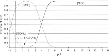
Eq. 1.2) of SiOH sites, the fraction of sites with positive, negative and zero charge, viz, θ
+, θ
- and θ
0 on SiO
2 can be calculated as a function of solution pH. The result of such a calculation is shown in
Figure 1.1 for SiO
2 using
K1 and
K2 values of 10
0.7 and 10
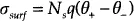
-3.9 respectively [4]. The surface charge density (coulombs per square meter),
at any particular pH is given by the expression:
where Ns represents the total number of surface sites per square meter, and q is the fundamental electronic charge (coulombs).
Figure 1.1 shows that the surface of SiO2 is positively charged at low pH and negatively charged at high pH. At a pH of ~1.5, the fraction of positive sites is equal to the fraction of negative sites. This pH is called the point of zero charge (PZC) [5]. It is worth noting that at the PZC while the fractions of positively charged and negatively charged sites may be equal, each fraction may not be 0.5. The PZC value is roughly equal to the average of pK1 and pK2. Reference [6] outlines surface charging theory with respect to wafer cleaning.
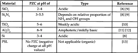
Oxides may be classified as acidic, basic, or amphoteric [7]. Acidic oxides are generally oxides of non-metals (e.g. SiO2, As2O3) that are dissolved by bases. By contrast, basic oxides (e.g. alkaline earth oxides such as MgO, FeO) are oxides of metals that are dissolved by acids. Oxides that show both acidic and basic properties are referred to as amphoteric oxides (e.g. Al2O3, SnO). Acidic oxides exhibit a low PZC while basic oxides exhibit higher PZC. For example, SiO2, an acidic material, exhibits a PZC close to a pH of 2 while Al2O3, a basic material, exhibits a PZC close to a pH of 9. Table 1.1 lists PZC of materials of interest to semiconductor processing.
Table 1.1 Point of zero charge of materials of interest to wafer cleaning
An acid- base mass titration technique is typically used to determine the PZC of materials. In this technique demonstrated by Schwarz, a suspension of oxide particles in an electrolyte is titrated with a standard acid/base solution [14]. The protonation/ deprotonation of the oxide surface causes the solution pH to increase/decrease from the original pH value. A mass balance from the added H
+/OH
- ions is then made to obtain the extent of adsorption of H
+ and OH
-. The surface charge density,
is given by:
where
and
are adsorption densities (moles per square meter) of
H+ and
OH-, respectively, and
F is the Faraday constant (96500 coulombs/gram equivalent).
The use of this technique is described in many papers [15–18] and only works well for samples with large surface areas such as particles. For materials with low surface areas such as oxide films, the pH change due to adsorption/desorption is too small to be accurately measured causing large errors in mass balance [19].
1.2.2 Surface Charging of Silicon Nitride Films in Aqueous Solutions
Silicon nitride films are most commonly deposited using a chemical vapor deposition (CVD) technique in which silane (SiH4) reacts with ammonia (NH3). Plasma-enhanced CVD (PECVD) forms SiNx and low pressure CVD (LPCVD) forms Si3N4. Consequently, silicon nitride films may contain up to 5–6 atomic % hydrogen, especially those formed with PECVD. As shown in Figure 1.2, these films typically have amine (-NHL,) surface groups, which depending on their pKa value can be protonated leading to the formation of positively charged sites [20]. The negative sites on the surface of nitride films have been postulated [21, 22] to be created by the reaction of surface amine groups with water forming silanol (Si-OH) followed by deprotonation to form negatively charged SiO- sites. The isoelectric point (defined in Section 1.2.3) of nitride films can vary widely depending on the hydrolytic strength of -NH2 groups, which in turn will depend on the solution pH, ionic strength, and temperature.