Optoelectronic sensors combine optical and electronic systems for numerous applications including pressure sensors, security systems, atmospheric particle measurement, close tolerance measurement, quality control, and more. This title provides an examination of the latest research in photonics and electronics in the areas of sensors.
- English
- ePUB (mobile friendly)
- Available on iOS & Android
eBook - ePub
Optoelectronic Sensors
About this book
Trusted by 375,005 students
Access to over 1.5 million titles for a fair monthly price.
Study more efficiently using our study tools.
Information
Chapter 1
Introduction to
Semiconductor Photodetectors 1
1.1. Brief overview of semiconductor materials
A semiconductor material is a continuous crystalline medium characterized by an energy band structure corresponding, in the case of an infinite crystal, to a continuum of states (which, in practice, means that the characteristic dimensions of the crystal are significantly larger than the lattice parameter of the crystal structure; this applies as long as the crystal dimensions are typically larger than a few dozen nanometers). In general terms, the energy structure of a semiconductor consists of a valence band corresponding to molecular bonding states and a conduction band representing the molecular antibonding states. The energy range lying between the top of the valence band and the bottom of the conduction band is known as the forbidden band, or more commonly the bandgap. An electron situated in the valence band is in a ground state and remains localized to a particular atom in the crystal structure, whereas an electron situated in the conduction band exists in an excited state, in a regime where it interacts very weakly with the crystalline structure. What differentiates semiconductors from insulators is essentially the size of the bandgap: we refer to semiconductors where the bandgap of the material is typically less than or equal to 6 eV, and to insulators when the bandgap is more than 6 eV: above this, the solar spectrum arriving on the Earth’s surface is unable to produce inter-band transitions of electrons situated in the valence band of the material. Semiconductor materials are mostly divided into two large classes: elemental semiconductors (group IV of the periodic table): silicon, germanium, diamond, etc. and compound semiconductors: IV-IV (SiC), III-V (GaAs, InP, InSb, GaN) and II-VI (CdTe, ZnSe, ZnS, etc.). Impurities can be introduced into the volume of the semiconductor material and can modify its electrical conduction properties, sometimes considerably. An impurity is known as a donor when it easily releases a free electron into the conduction band. The characteristic energy level of the impurity is therefore in the bandgap, slightly below the conduction band. For example, in the case of compound semiconductors in group IV of the periodic table such as silicon, the main donor impurities are those which, being from group V of the periodic table (arsenic, phosphorous, etc.), are substituted in place of a silicon atom in the crystal structure: since silicon is tetravalent, these atoms naturally form four covalent bonds with the silicon atoms around them, and also easily give up their surplus electron to the crystal structure. These electrons become free to move, subject to a weak activation energy provided by thermal agitation. In this case we refer to n-type doping. In the case of silicon, a group III element incorporated into the crystal structure of silicon naturally forms three covalent bonds around it, and then completes its own outer-shell electronic structure by capturing an electron from its fourth nearestneighbor silicon atom, again subject to a weak thermal activation energy. Such an impurity is known as an acceptor, and doping with acceptors is known as p-type doping. A hole carrying a positive elementary charge and corresponding to a vacant energy state in the valence band is therefore left in the crystal structure of the silicon. In the case of III-V composites, the donors are mostly atoms from group IV (silicon) substituted in place of group III elements, or group VI elements (S, Se, Te) substituted in place of group V elements, and acceptors are group II (zinc, magnesium) substituted in place of group III elements. In the case of II-VI composites, the most commonlyencountered donors belong to group VII (chlorine, etc.) substituted in place of group VI elements, and acceptors belong to either group I (lithium, etc.) or to group V (nitrogen, arsenic, phosphorous, etc). In this last case, the group V element is substituted in place of a group VI element in the semiconductor crystal structure, whereas group I acceptors are substituted in place of group II elements. The chemical potential, or Fermi energy, of an intrinsic semiconductor (i.e. one free from n and p impurities) is found in the middle of the bandgap of the material. When a moderate n-type doping is added, the Fermi level rises from the middle of the bandgap towards the conduction band, by an increasing amount as the level of doping rises. When the level of n-type doping becomes large, the Fermi level can cross the bottom of the conduction band and be found inside this band (Mott transition). The semiconductor then behaves like a metal and for this reason is called a semi-metal. In this case it is referred to as degenerate. In the case of p-type doping, the semiconductor is said to be degenerate when the Fermi level is below the top of the valence band.
1.2. Photodetection with semiconductors: basic phenomena
Photodetection in semiconductors works on the general principle of the creation of electron-hole pairs under the action of light. When a semiconductor material is illuminated by photons of an energy greater than or equal to its bandgap, the absorbed photons promote electrons from the valence band into excited states in the conduction band, where they behave like free electrons able to travel long distances across the crystal structure under the influence of an intrinsic or externally-applied electric field. In addition, the positively-charged holes left in the valence band contribute to electrical conduction by moving from one atomic site to another under the effects of the electric field. In this way the separation of electron-hole pairs generated by the absorption of light gives rise to a photocurrent, which refers by definition to the fraction of the photogenerated free charge-carriers collected at the edges of the material by the electrodes of the photodetecting structure, and whose intensity at a given wavelength is an increasing function of the incident light intensity. On this level we can distinguish between two large categories of photodetectors based on the nature of the electric field, which causes the charge separation of photogenerated electron-hold pairs: photoconductors, which consist of a simple layer of semiconductor simply with two ohmic contacts, where the electric field leading to the collection of the charge-carriers is provided by applying a bias voltage between the contacts at either end, and photovoltaic photodetectors, which use the internal electric field of a p-n or Schottky (metalsemiconductor) junction to achieve the charge separation. This last term covers p-n junction photodetectors (photovoltaic structures consisting of a simple p-n junction, and p-i-n photodetectors which include a thin layer of semiconductor material between the p and n region which is not deliberately doped), as well as all Schottky junction photodetectors (Schottky barrier photodiodes and metalsemiconductor-metal (MSM) photodiodes).
We will now briefly introduce the main physical concepts at the root of the operation of the different semiconductor photodetector families. Here the emphasis is placed on a phenomenological description of the working mechanisms of the devices in question; the corresponding formalism has been deliberately kept to an absolute minimum in the interests of clarity and concision.
1.3. Semiconductor devices
Photoconductors represent the simplest conceivable type of photodetector: they consist of a finite-length semiconductor layer with an ohmic contact at each end (Figure 1.1). A fixed voltage of magnitude VB is applied between the two end contacts, in such a way that a bias current IB flows through the semiconductor layer, simply following Ohm’s law. The active optical surface is formed from the region between the two collection electrodes. When it is illuminated, the photogenerated changes produced under the effect of the applied electric field lead to a photocurrent IPH which is added to the bias current, effectively increasing the conductivity of the device.
Figure 1.1. Diagram of a photoconducting device
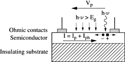
The main point of interest in a photoconducting device is its increased gain, the response of photoconductors being typically several orders of magnitude greater than that of photovoltaic detectors for a given material. On the other hand, its other operational parameters (bandwidth, UV/visible contrast, infrared sensitivity) are generally below that of other types of photodetectors, which often greatly limits the scope of its potential applications (this is particularly the case for photoconductors based on III-V nitrides, as we will see later on).
1.4. p-n junctions and p-i-n structures
In p-n diodes, the metallurgical linkage of a region of a p-type doped semiconductor and a region of n-type doping forms a p-n junction, where the joining of the Fermi levels in equilibrium mostly occurs through a flow of charge between the n and p regions. In equilibrium we therefore find a region with no free charge carriers immediately around the junction, similar to a charged capacitor, where there are, on the n side, positively ionized donors and, on the p side, negatively ionized acceptors (this zone is known as the space charge region (SCR), where ionized donors and acceptors provide fixed charges). The presence of charged donors and acceptors produces an electric field in that region which curves the energy bands and, in equilibrium, forms an energy barrier between the two regions: the bottom of the conduction band and the top of the valence band on t...
Table of contents
- Cover
- Title Page
- Copyright
- Preface
- Chapter 1: Introduction to Semiconductor Photodetectors
- Chapter 2: PIN Photodiodes for the Visible and Near-Infrared
- Chapter 3: Avalanche Photodiodes
- Chapter 4: Phototransistors
- Chapter 5: Metal-Semiconductor-Metal Photodiodes
- Chapter 6: Ultraviolet Photodetectors
- Chapter 7: Noise in Photodiodes and Photoreceiver Systems
- List of Authors
- Index
Frequently asked questions
Yes, you can cancel anytime from the Subscription tab in your account settings on the Perlego website. Your subscription will stay active until the end of your current billing period. Learn how to cancel your subscription
No, books cannot be downloaded as external files, such as PDFs, for use outside of Perlego. However, you can download books within the Perlego app for offline reading on mobile or tablet. Learn how to download books offline
Perlego offers two plans: Essential and Complete
- Essential is ideal for learners and professionals who enjoy exploring a wide range of subjects. Access the Essential Library with 800,000+ trusted titles and best-sellers across business, personal growth, and the humanities. Includes unlimited reading time and Standard Read Aloud voice.
- Complete: Perfect for advanced learners and researchers needing full, unrestricted access. Unlock 1.5M+ books across hundreds of subjects, including academic and specialized titles. The Complete Plan also includes advanced features like Premium Read Aloud and Research Assistant.
We are an online textbook subscription service, where you can get access to an entire online library for less than the price of a single book per month. With over 1.5 million books across 990+ topics, we’ve got you covered! Learn about our mission
Look out for the read-aloud symbol on your next book to see if you can listen to it. The read-aloud tool reads text aloud for you, highlighting the text as it is being read. You can pause it, speed it up and slow it down. Learn more about Read Aloud
Yes! You can use the Perlego app on both iOS and Android devices to read anytime, anywhere — even offline. Perfect for commutes or when you’re on the go.
Please note we cannot support devices running on iOS 13 and Android 7 or earlier. Learn more about using the app
Please note we cannot support devices running on iOS 13 and Android 7 or earlier. Learn more about using the app
Yes, you can access Optoelectronic Sensors by Didier Decoster, Joseph Harari, Didier Decoster,Joseph Harari in PDF and/or ePUB format, as well as other popular books in Technology & Engineering & Electrical Engineering & Telecommunications. We have over 1.5 million books available in our catalogue for you to explore.