- English
- ePUB (mobile friendly)
- Available on iOS & Android
eBook - ePub
Nanostructured Conductive Polymers
About this book
Providing a vital link between nanotechnology and conductive polymers, this book covers advances in topics of this interdisciplinary area. In each chapter, there is a discussion of current research issues while reviewing the background of the topic. The selection of topics and contributors from around the globe make this text an outstanding resource for researchers involved in the field of nanomaterials or polymer materials design. The book is divided into three sections: From Conductive Polymers to Nanotechnology, Synthesis and Characterization, and Applications.
Trusted by 375,005 students
Access to over 1.5 million titles for a fair monthly price.
Study more efficiently using our study tools.
Information
Part One
1
History of Conductive Polymers
1.1 Introduction
It is generally recognized that the modern study of electric conduction in conjugated polymers began in 1977 with the publication by the group at the University of Pennsylvania [1] describing the doping of polyacetylene. Although there was some prior work dating back to World War II (see the review by Hush [2]) and even reports of electrochemical synthesis the nineteenth century [3], the Nobel Committee recognized the seminal contribution of Heeger [4], MacDiarmid [5] and Shirakawa [6] by awarding them the Nobel Prize for Chemistry in 2000. Shirakawa, who was based at the Tokyo Institute of Technology, had been visiting the lab of his collaborators at Pennsylvania at the time of the breakthrough research.
The story of polyacetylene is an example of a fortunate confluence of circumstances that is often under-appreciated in the history of scientific progress. In the 1970s, there was worldwide interest in the unique properties of materials with such a high degree of anisotropy that they can be considered one-dimensional (1D) systems. The Pennsylvania group, of which I was privileged to be a member until 1975, was jointly led by a chemist, Tony Garito, and a physicist, Alan Heeger, and was recognized worldwide as a primary center for that field. Early focus was on the study of charge-transfer salts, in which planar, conjugated, small molecules were stacked like poker chips. Experiments revealed a Peierls transition [7,8] and suggested the observation of Fro¨lich superconductivity [9,10]. The emphasis then shifted to linear polymers as chemist, Alan MacDiarmid, entered into a collaboration with Heeger, to examine poly(sulfur-nitride), a crystalline solid, consisting of chains of alternating sulfur and nitrogen atoms, that exhibits metallic conduction [11] down to liquid helium temperatures, and has a superconducting transition at 0.26 K [12].
In the midst of this research, MacDiarmid was traveling in Japan and visited the laboratory of Hideki Shirakawa who was studying the Ziegler–Natta-catalyzed polymerization of acetylene. Standard practice was to use a concentration of the organometallic catalyst at the millimolar level. It is a catalyst after all. These low concentrations led to the infamous ‘insoluble, intractable, black precipitate,’ but Shirakawa had discovered that with concentrations closer to molar, he obtained a shiny ‘metallic’ film coating the wall of the reaction vessel. MacDiarmid returned to Pennsylvania, where he and Heeger quickly arranged to invite Shirakawa for a sabbatical visit.
The pieces were all in place. Scientifically, it was understood that pristine polyacetylene is a Peierls semiconductor, as evidenced by its bond-alternating structure; it was known that charge transfer to molecular donors or acceptors would result in partially filled bands and that the resulting incommensurability of the Fermi wave-vector would destabilize the Peierls phase. The interdisciplinary team had the ideal expertise: the chemists, led by Shirakawa and MacDiarmid, brought their synthetic expertise to the preparation of the polymer films; the physicists, led by Heeger and post-doc C. K. Chiang, brought physical measurement and interpretation of material properties, not just electrical conductivity, but also structural and spectroscopic. Together, they applied vapor-phase doping of molecular acceptors (halogens) and a donor (ammonia).
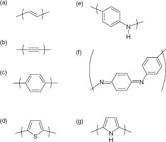
The publication by Chiang et al. [1] led to a huge surge in interest in ‘synthetic metals.’ In less than a decade, most of the monomer building blocks that we know today had been identified and many procedures for polymeric synthesis had been established. The chemical structures are illustrated in Figure 1.1. (In the nomenclature used in Figure 1.1, polyacetylene would be called polyvinylene. This is because some – ‘common’ – names derive from the compound that is polymerized, while others, more correctly according to IUPAC conventions, use the monomeric unit in the product polymer.)
An interesting sociological aspect of the research on conjugated polymers has been the evolving target for technological application, and hence emphasis on particular physical properties, that has motivated the research in the ensuing 30 years. Initially, and through the early 1980s, high electrical conductivity was the primary driving force. There were suggestions to replace (copper) electrical wiring in everything from printed circuit boards to home, and even grid, power distribution with inexpensive, light-weight polymeric conductors. As issues of processability, limits on conductivity, and environmental stability became more apparent these grand schemes fell by the wayside. Nevertheless, in certain niche applications, electrical conductivity is the primary attribute. For example, antistatic coatings are important in many textiles and in the roll-to-roll processing of polymer webs. Photographic film is a good example of the latter application and is the reason that Bayer initiated, in conjunction with Agfa, their development of the Baytron series of products based on poly(ethylenedioxythiophene) (PEDOT) doped with poly(styrene sulphonate) PSS. (PEDOT-PSS is currently marketed by H. C. Starck Corp. as their Clarion line of conductive coatings.)
When the Holy Grail of copper replacement receded over the horizon, the emphasis in the late 1980s and early 1990s shifted to the optical properties. Since there is typically a large oscillator strength in the HOMO–LUMO transition of undoped conjugated polymers, they are often highly colored and fluorescent. At that time there was great interest in nonlinear optics, as researchers were developing new materials, both organic and inorganic, for application in optical switches, modulators and the like. It was experimentally demonstrated [13] and theoretically understood [14,15] that many conjugated polymers also possess extremely high third-order optical nonlinearity. Although much interesting science emerged from this line of research, to my knowledge no technology is based on it.
Figure 1.1 Chemical structures for monomers of the conjugated polymers discussed in this chapter: (a) vinylene (the repeat unit of polyacetylene); (b) ethynylene (polydiacetylene is alternating vinylene-ethynylene); (c) phenylene; (d) thiophene; (e) leucoemeraldine form of polyaniline; (f) pernigraniline form of polyaniline (the number of protons can vary between the two limits); (g) pyrrole
Second-order nonlinearity and electro-optic response are much more amenable to device application. There are few conjugated polymers with intrinsic second-order non-linearity, since homopolymers and alternating copolymers tend to have a center of symmetry. (This is not necessarily always so, since head-to-tail polymerization of an asymmetric monomer does not have mirror symmetry.) In 1990, the Cambridge group under the leadership of Richard Friend was investigating the electro-optic response of poly(phenylene vinylene). The story goes (I have heard several versions, probably with some embellishment) that graduate student Jeremy Burroughes had turned off the lab lights in order to minimize stray light, and applied a dc voltage to a sandwich-structured device – just the conditions required to observe the resulting electroluminescence. Of course, the publication of this observation [16] spawned an enormous worldwide research effort to optimize the materials and device structures (polymer light-emitting diodes or PLEDs) for use in flat-panel displays, signage and lighting.
The semiconductive properties of conjugated polymers are also exploited for application in thin-film organic field-effect transistors (OFETs). The earliest materials examined were polyacetylene [17], polythiophene [18], and an oligomer of thiophene [19]. In these devices the polymer forms the channel between the source and drain electrodes of the device. The number of charge carriers in the channel is modulated by the voltage applied to the gate electrode. The conductance of the channel is proportional to the number of charge carriers and to their mobility. Hence, charge-carrier mobility is the primary metric in screening materials for use in OFETs. As several other chapters in this volume discuss in detail, polymer morphology at the nanoscale plays a crucial role in dictating the mobility. In any conductor a high degree of order is essential to achieve high mobility, since disorder leads to scattering, trapping at defects, and localization. However, as discussed by Kline et al. [20] among others, highly crystalline polymers are not necessarily ideal, because the crystallites are typically much smaller than the channel length, in which case the mobility is limited by transfer across grain boundaries. It seems preferable to have a high degree of polymer chain alignment, but with few grain boundaries and with many chains bridging between adjacent domains. Nano-morphology is key.
Another application which relies on the optical and semiconducting properties of conjugated polymers is solar-energy conversion. In this case, each photon of solar radiation is absorbed to generate an exciton – a bound electron–hole pair. The onset of absorption is below the HOMO–LUMO gap by an energy corresponding to the exciton binding energy. In contrast to many inorganic semiconductors used in solar cells, the exciton binding energy in conjugated polymers is several tenths of an electronvolt and therefore many times thermal energy (kT) at ambient temperature. Therefore excitons in conjugated polymers do not readily dissociate to create free electrons and holes. Excitonic solar cells rely on a hetero-junction to dissociate the excitons. In this device structure, an electron-transport material (n-type) is adjacent to a hole-transport material (p-type). If the energy level offsets (HOMO and LUMO of the n- and p-type materials) are sufficient compared to the binding energy, the exciton may dissociate at the interface. The exciton may be created in either the n- or p-type material or both, the difference being the absorption spectra and magnitudes of the binding energy.
Here again, nano-morphology plays a key role. The exciton has a characteristic lifetime, dictated by the sum of its radiative (re-emission) and non-radiative (heat-producing) decay rates. It is also mobile, diffusing through one of the polymeric semiconductors with a characteristic diffusivity. If the exciton lives long enough to diffuse to the n–p interface, high carrier-generation efficiency can be achieved. Since the exciton diffusion length in conjugated polymers is typically of the order of 5–10 nm, the n- and p-type materials must be blended at this length scale. Such ‘bulk heterojunctions’ were first demonstrated by the Santa Barbara [21] and Cambridge [22] groups.
There is an additional constraint on the nature of the mixing, namely that the hole-transporting p-type phase be continuous to the cathode, while the electron-transporting n-type phase connect to the anode. Controlling the morphology of such bi-continuous networks is the goal of recent research on self-assembled block copolymers.
Most of this volume is devoted to the characterization and application of doped conjugated polymers, i.e. to their highly conducting ‘metallic’ state. I have touched upon some of the issues relating to the nano-morphology of undoped conjugated polymers, and to their application as semiconductors, because it is usually helpful to understand properties of the ‘pristine’ material prior to analyzing the effect of dopants. The remainder of this chapter is divided into sections devoted to, respectively, the work that preceded the Pennsylvania publication (‘archeology and prehistory’), its immediate impact (‘the dawn of the modern era’), and the ‘materials revolution,’ which brought careful refinement of synthesis and processing, and thereby enables today’s applications.
1.2 Archeology and Prehistory
Today’s conductive polymer workhorses are primarily derivatives of polypyrrole, polyani-line and polythiophene. Each of these was known to the chemical community long before the work on doping of polyacetylene. The earliest publication that I am aware of concerns the oxidative polymerization of ‘indigo’ (i.e. aniline) by nitric acid [23]. This was soon, at the pace of ninteenth century science, followed by a paper ‘On the production of a blue substance by the electrolysis of sulphate of aniline’ [3]. The background was the industrial revolution, when chemists were exploring the usefulness of coal by-products and just post-Faraday, electrochemistry was in its infancy. Aniline was particularly interesting because it was a reagent in the synthesis of many of the dyes that we associate with the deep crimsons and purples of the Victorian era. Fritsche [23] and Letheby [3] had undoubtedly synthesized some form of polyaniline, long before the concept of linear polymerization [24,25], and long before the concept of frontier orbitals, which is so important in understanding organic c...
Table of contents
- Cover Page
- Title Page
- Copyright
- Preface
- Foreword
- List of Contributors
- Part One
- Part Two
- Part Three
- Index
Frequently asked questions
Yes, you can cancel anytime from the Subscription tab in your account settings on the Perlego website. Your subscription will stay active until the end of your current billing period. Learn how to cancel your subscription
No, books cannot be downloaded as external files, such as PDFs, for use outside of Perlego. However, you can download books within the Perlego app for offline reading on mobile or tablet. Learn how to download books offline
Perlego offers two plans: Essential and Complete
- Essential is ideal for learners and professionals who enjoy exploring a wide range of subjects. Access the Essential Library with 800,000+ trusted titles and best-sellers across business, personal growth, and the humanities. Includes unlimited reading time and Standard Read Aloud voice.
- Complete: Perfect for advanced learners and researchers needing full, unrestricted access. Unlock 1.5M+ books across hundreds of subjects, including academic and specialized titles. The Complete Plan also includes advanced features like Premium Read Aloud and Research Assistant.
We are an online textbook subscription service, where you can get access to an entire online library for less than the price of a single book per month. With over 1.5 million books across 990+ topics, we’ve got you covered! Learn about our mission
Look out for the read-aloud symbol on your next book to see if you can listen to it. The read-aloud tool reads text aloud for you, highlighting the text as it is being read. You can pause it, speed it up and slow it down. Learn more about Read Aloud
Yes! You can use the Perlego app on both iOS and Android devices to read anytime, anywhere — even offline. Perfect for commutes or when you’re on the go.
Please note we cannot support devices running on iOS 13 and Android 7 or earlier. Learn more about using the app
Please note we cannot support devices running on iOS 13 and Android 7 or earlier. Learn more about using the app
Yes, you can access Nanostructured Conductive Polymers by Ali Eftekhari in PDF and/or ePUB format, as well as other popular books in Tecnologia e ingegneria & Scienza dei materiali. We have over 1.5 million books available in our catalogue for you to explore.