![]()
Chapter 1
ESD Design Synthesis
1.1 ESD Design Synthesis and Architecture Flow
In the ESD design synthesis process, there is a flow of steps and procedures to construct a semiconductor chip [1–13]. In many cases, the floorplanning process is a function of the type of semiconductor chip. The following design synthesis procedure is an example of an ESD design flow needed for semiconductor chip implementations:
- I/O, Domains and Core Floorplan: Define floorplan of regions of cores, domains, and peripheral I/O circuitry.
- I/O Floorplan: Define area and placement for I/O circuitry.
- ESD Signal Pin Floorplan: Define ESD area and placement.
- ESD Power Clamp Network Floorplan: Define ESD power clamp area and placement for a given domain.
- ESD Domain-to-Domain Network Floorplan: Define ESD networks between the different chip domains area and placement for a given domain.
- ESD Signal Pin Network Definition: Define ESD network for the I/O circuitry.
- ESD Power Clamp Network Definition: Define ESD power clamp network within a power domain.
- Power Bus Definition and Placement: Define placement, bus width, and resistance requirements for the power bus.
- Ground Bus Definition and Placement: Define placement, bus width, and resistance requirements for the ground bus.
- I/O to ESD Guard Rings: Define guard rings between I/O and ESD networks.
- I/O Internal Guard Rings: Define guard rings within the I/O circuitry.
- I/O External Guard Rings: Define guard rings between I/O circuitry and adjacent external circuitry.
1.1.1 Top-Down ESD Design
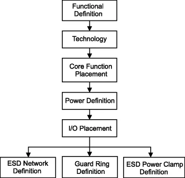
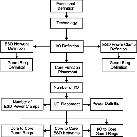
In the ESD design synthesis, the implementation can be thought of as a “top-down ESD design” process. Figure 1.1 is an example of a “top-down ESD design flow.” In the ESD design synthesis process, there is a flow of steps and procedures to construct a semiconductor chip. In my experience, in the planning stages of a semiconductor chip, the circuit team leader addresses the ESD design synthesis from a procedure as shown. With a “top-down ESD design synthesis” the integration, placement, sizing, and requirements are addressed. This process will be independent of whether the semiconductor chip is for digital logic [1–7, 11], analog design [14, 31–33], power electronics [26–30, 35–38], or radio frequency applications [8, 39–41].
1.1.2 Bottom-Up ESD Design
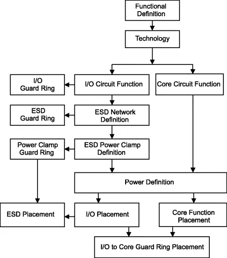
In the ESD design synthesis, the implementation can also be addressed as a “bottom-up ESD design” process. Figure 1.2 is an example of a “bottom-up ESD design flow.” In a bottom-up ESD design synthesis process, the circuits are defined, and the corresponding ESD networks.
One of the difficulties of ESD and the latchup design synthesis process is that the ESD design synthesis requires some “top-down” procedures, some “bottom-up” thinking, and integration. This will become more apparent throughout this text.
1.1.3 Top-Down ESD Design – Memory Semiconductor Chips
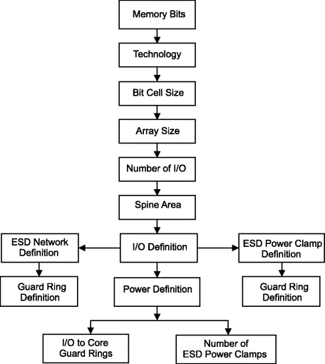
In the ESD design synthesis of a memory chip, the thought process is a “top-down ESD design” process, with the floorplanning driven by the array region. These designs are “array-dominated” designs, with the focus on the array [7]. The I/O region is limited in physical area, and the architecture is driven by the number of output pins, how to integrate it with the packaging, and how to support the I/O and ESD in the least amount of space. Figure 1.3 is an example of a “top-down ESD design flow” for a memory chip.
1.1.4 Top-Down ESD Design – ASIC Design System
In the ESD design synthesis of an applications-specific IC (ASIC) architecture, the procedure for the ESD design integration is significantly different. In the ASIC environment, the chip size, the number of I/O, and its ESD integration is dependent on the chip size. In this “top-down” methodology, the number of I/O, supported bus locations, placement of the I/O cells, integration of the ESD elements, and power are all synthesized in a different flow. Figure 1.4 is an example of a “top-down ESD design flow” for an ASIC methodology.
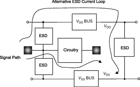
1.2 ESD Design – The Signal Path and the Alternate Current Path
In semiconductor chip design, the role of a semiconductor chip is to receive a signal, process the signal, and transmit the signal.
In ESD design synthesis, the role of the ESD network solution is to establish an alternate current path to avoid damage along the signal path that impacts its function or operation characteristics [7, 11]. As a result, simplistically, the ESD network must transmit the ESD current out of the sensitive signal path to an alternative path or current loop. This is achieved by diverting the ESD current to the power grid, or the ground plane. The fundamental requirements along the alternative current path are as follows:
- An alternative current path must exist between any signal pin and any grounded reference (e.g., signal pin, power pin, ground pin).
- An ESD element must divert the ESD current to the power plane or ground plane.
- An ESD element must be able to transmit the ESD current to the power rail or ground rail without damage (to some specification level).
- The power rail and ground rail must be able to source the ESD current without damage (to some specification level).
- The alternative current path must achieve the ESD current discharge to the grounded reference to some specification level prior to damage along the signal path.
To achieve this objective, there are some conditions on the alternative current path:
- ESD networks are required to address both positive and negative polarity events.
- The ESD network must have low turn-on voltage and low resistance prior to destruction of the circuitry along the signal path.
- The power grid and the ground rail resistance must be sufficiently low to avoid IR voltage drops.
- Bi-directional electrical connectivity must exist, providing an alternative current path between all independent rails through ESD networks, or other means (e.g., circuitry, inductors, bond wires, packaging, etc.).
Figure 1.5 shows an example of a semiconductor high-level schematic of the chip architecture. The figure highlights the signal path and the alternative ESD current path created by the ESD networks.
1.3 ESD Electrical Circuit and Schematic Architecture Concepts
In this section, discussion of ESD from a chip architecture, and the electrical schematic viewpoint will be shown. What are the ideal characteristics that we are looking for from an ESD network? What are the ideal characteristics from a frequency domain perspective? How is the chip architecture related to the testing procedure and the events that occur in a real chip?
1.3.1 The Ideal ESD Network and the Current–Voltage DC Design Window
The DC I–V characteristics may determine the “on” and “off” characteristics of the ESD network during functional operation, and its ESD effectiveness as an ESD network to protect other circuitry. An ideal ESD network has the following characteristics [7, 11]:
- The ESD device, circuit, or network is “off” during the DC functional regime between signal levels between the most negative power supply voltage and the most positive power supply (associated with the signal pin).
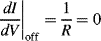
- The ESD network has an “infinite resistance” when in the “off” state, which can be expressed as
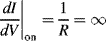
The ESD network is “on” during voltage excursions that undershoot below the most negative power supply, or voltage excursions that overshoot the most positive power supply (during ESD testing).
- The ESD network has a “zero resistance” when
The ESD network operation extends beyond the “electrical safe-operation area” (electrical SOA) in DC voltage level or DC current level [26–30].
- The ESD network operation does not extend beyond a “thermal safe-operation area” (thermal SOA) in DC voltage level or DC current level [26–30].
- The ESD network operation does not reach the current-to-failure, voltage-to-failure, or power-to-failure prior to the ESD specification level objective [15–30].
ESD networks can consist of I–V characteristics of the following form:
- Step function I–V characteristics.
- S-type I–V characteristics.
- N-type I–V characteristics.
Step function I–V characteristics have a single “off” state as the structure is biased. At some voltage value, the device is “on.” For example, a diode element has a step function I–V characteristic and is suitable for ESD protection. In the case of a diode element...