![]()
CHAPTER 1
CLOCK SIGNAL IN ELECTRONIC SYSTEMS
1.1 THE SIGNIFICANCE OF CLOCK SIGNAL
1.1.1 Clock Signal
In modern electronic-driven society, our everyday lives are supported by various kinds of electronic devices. At home, TV, computer, audio system, game machine, and digital camera are indispensable for our entertainment and relaxation. Away from home, mobile phones keep us connected with the world all the time. On the road, automobiles and airplanes with countless built-in electronic devices make them safe to be driven/flown and comfortable to ride in. At work, we spend most of our time dealing with the computer, fax machine, copier, printer, projector, etc. Without these electronic devices, people’s lives would be totally different; human society would regress many years in standard of living. Electronic devices have already penetrated into all aspects of our lives.
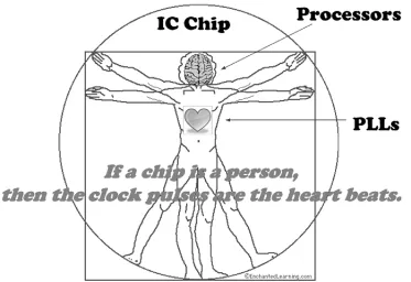
When in operation, almost all electronic devices rely on a very important signal: the clock. This is simply due to the fact that electronic devices are made of very-large-scale-integration (VLSI) chips, which are primarily designed on the synchronous principle. For any chip, simple or complex, its designed functionality is achieved by millions of events that occur inside it. These events do not happen randomly but in a predetermined, orderly sequence. The clock signal is the conductor of the orchestra to produce harmony. For successful operation in a large chip, many clock signals (as many as hundreds) could be required simultaneously. Usually, phase-locked loop (PLL) is used on-chip to generate these crucial clock signals. If a VLSI chip could be treated as a person and the on-chip processor were regarded as the brain, then the clock pulse is the heartbeat, the clock signal is the blood, and the clock distribution network (clock tree) is the vessel. This analogy is graphically demonstrated in Fig. 1.1.
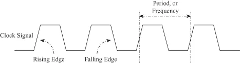
In the field of VLSI circuit design, the clock signal is an electrical pulse train of square waveform as shown in Fig. 1.2. It has two distinguishable voltage levels: high and low. The basic unit in this pulse train comprises one occurrence of high level voltage and one occurrence of low level voltage. The transitions between the low-to-high and high-to-low are termed the clock edges. They are called “rising edge” and “falling edge,” respectively. The length-in-time used by this basic unit is defined as the clock period; its inversion is the frequency that is often used by people to gauge the working speed of an electronic device.
One of the most important characteristics of the clock signal is that the basic unit, often called the cycle, has to be able to repeat itself indefinitely. In other words, in this pulse train, every cycle has to be exactly the same. This is because that clock signal is the driver of the chip. The billions of operations (can also be viewed as events) inside a VLSI chip are all coordinated by clock signal. Structurally, the circuit inside the chip is designed in such way that these operations are triggered by either the rising edge or the falling edge, or both, of the clock signal. Therefore, it is essential that the occurrences of these edges in time are precisely predictable. The easiest way of achieving this goal is to make every cycle the same. A clock signal with this predictability in its waveform has enabled an important VLSI circuit design method: synchronous design. The synchronous design methodology is a milestone technology that allows the VLSI chip design industry to make great strides.
The physical medium inside the electronic circuit is electrical voltage or current. The electronic circuit is naturally suitable for handling the magnitude of this medium. (In all VLSI chips, information is represented through the magnitude of this medium.) By manipulating the magnitude, VLSI chips can process information and produce result for us to use. Manipulating the medium’s magnitude for representing information is natural for an electronic circuit, since magnitude is directly proportional to the number of electronics flowing inside electronic devices. On the other hand, an electronic circuit is not naturally born for managing the other important variable: time. Instead, electronic systems use voltage transition to represent timing information. Therefore, it is not an easy task to generate the period of the basic unit (clock cycle) any way you want. It usually requires external help of a timing reference source, such as a mechanical crystal oscillator. Then, a special circuitry of PLL is used to produce other time scales based on this precise reference. This field of work is called frequency synthesis, and it is one of the most actively researched and engineered areas in VLSI circuit design.
1.1.2 The Aim of This Book
Due to the difficulty of using electronic circuits to manipulate the time scale, the capability of PLLs is limited. In many cases, it is extremely difficult and costly for the clock circuit design engineer to produce the clock frequencies that the system engineer prefers. Most of the time, the system engineer has to use whatever frequencies the PLL circuit designer is able to offer. Moreover, when a PLL is used as the clock source, it is difficult to switch from one frequency to another in a short time (a short time in comparison to the clock period). Consequently, these problems have limited our options for designing better and cheaper electronic products.
Throughout the history of frequency synthesis development, there are three distinguished approaches: direct analog synthesis, direct digital frequency synthesis (DDFS), and PLL-based indirect frequency synthesis. Among these, the PLL-based method is the most popular one for on-chip clock generation. There are several styles in the PLL-based approach: integer-N PLL, fractional-N PLL, sigma-delta fractional-N PLL, and all digital PLL (ADPLL). All the aforesaid techniques are built around one basic consensus: constructing the clock waveform with equal lengths in time for all the cycles. In other words, the basic unit of the clock waveform is repeatable; all the units have to be exactly the same. This feature is ideal for the clock that is being used as the driver signal for chip operation because the location in time of every edge is precisely predictable. Unfortunately, this is also the single most influencing factor that makes the task of clock generation (frequency synthesis) difficult.
History shows that major science and technology advancements often start with adventurous thinking. Breakthroughs usually happen when traditional thinking is detoured. Moreover, most of the time, crucial advancement is initialized at the conceptual level. After a long period of time sticking with the belief that “all cycles shall have same length-in-time,” it is worth focusing our attention back to the two fundamental issues:
1. In the field of electronic circuit design, what does frequency mean?
2. In circuit design practice, how is the clock signal used?
The process of searching the answers for these two questions has induced the formal introduction of the time-average-frequency concept (Xiu 2008a). This rigorously formed concept lays down the foundation for a new frequency synthesis technique: flying-adder direct period synthesis architecture. Together, time-average-frequency and flying-adder architecture are the two cornerstones of a new circuit component: digital-to-frequency converter (Xiu 2008b). These breakthrough innovations, as illustrated in Fig. 1.3, are ...