eBook - ePub
Organic Thin Film Transistor Integration
A Hybrid Approach
- English
- ePUB (mobile friendly)
- Available on iOS & Android
eBook - ePub
Organic Thin Film Transistor Integration
A Hybrid Approach
About this book
Research on organic electronics (or plastic electronics) is driven by the need to create systems that are lightweight, unbreakable, and mechanically flexible. With the remarkable improvement in the performance of organic semiconductor materials during the past few decades, organic electronics appeal to innovative, practical, and broad-impact applications requiring large-area coverage, mechanical flexibility, low-temperature processing, and low cost. Thus, organic electronics appeal to a broad range of electronic devices and products including transistors, diodes, sensors, solar cells, lighting, displays, and electronic identification and tracking devices A number of commercial opportunities have been identified for organic thin film transistors (OTFTs), ranging from flexible displays, electronic paper, radio-frequency identification (RFID) tags, smart cards, to low-cost disposable electronic products, and more are continually being invented as the technology matures. The potential applications for "plastic electronics" are huge but several technological hurdles must be overcome. In many of these applications, transistor serves as a fundamental building block to implement the necessary electronic functionality. Hence, research in organic thin film transistors (OTFTs) or organic field effect transistors (OFETs) is eminently pertinent to the development and realization of organic electronics. This book presents a comprehensive investigation of the production and application of a variety of polymer based transistor devices and circuits. It begins with a detailed overview of Organic Thin Film Transistors (OTFTs) and discusses the various possible fabrication methods reported so far. This is followed by two major sections on the choice, optimization and implementation of the gate dielectric material to be used. Details of the effects of processing on the efficiency of the contacts are then provided. The book concludes with a chapter on the integration of such devices to produce a variety of OTFT based circuits and systems. The key objective is to examine strategies to exploit existing materials and techniques to advance OTFT technology in device performance, device manufacture, and device integration. Finally, the collective knowledge from these investigations facilitates the integration of OTFTs into organic circuits, which is expected to contribute to the development of new generation of all-organic displays for communication devices and other pertinent applications. Overall, a major outcome of this work is that it provides an economical means for organic transistor and circuit integration, by enabling the use of a well-established PECVD infrastructure, while not compromising the performance of electronics. The techniques established here are not limited to use in OTFTs only; the organic semiconductor and SiNx combination can be used in other device structures (e.g., sensors, diodes, photovoltaics). Furthermore, the approach and strategy used for interface optimization can be extended to the development of other materials systems.
Trusted by 375,005 students
Access to over 1.5 million titles for a fair monthly price.
Study more efficiently using our study tools.
Information
1
Introduction
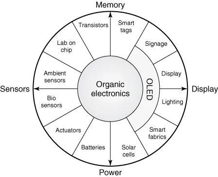
Organic semiconductor technology has attracted considerable research interest in view of its great promise for large area, low-end, lightweight, and flexible electronics applications [1]. Owing to their processability advantages and unique physical (i.e., electrical, optical, thermal, and magnetic) properties, organic semiconductors can bring exciting new opportunities for broad-impact applications requiring large-area coverage, mechanical flexibility, low-temperature processing, and low cost. Thus, organic semiconductors have appeal for a broad range of devices including transistors, diodes, sensors, solar cells, and light-emitting devices. Figure 1.1 depicts a number of application domains that can benefit from the versatility of organic electronics technology [2]. Since their proof of concept in the 1980s, the impressive development in organic semiconductor materials has led to performance properties that are competitive with amorphous silicon (a-Si), increasing their suitability for commercial applications [3].
Figure 1.1 A broad range of products and technologies inspired by organic electronics [2].
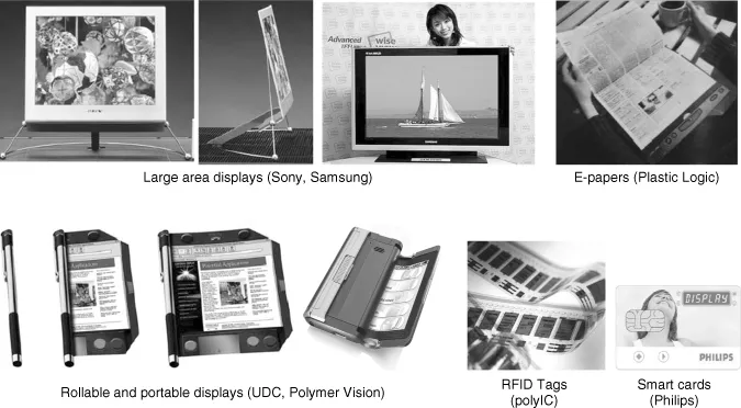
The transistor is a fundamental building block for all modern electronics; transistors based on organic semiconductors as the active layer are referred to as organic thin film transistors (OTFTs). A number of commercial opportunities have been identified for OTFTs, including flat panel active-matrix liquid crystal displays (LCDs) or active matrix organic light-emitting diode displays (AMOLEDs), electronic paper (e-paper), low-end data storage such as smart cards, radio-frequency identification (RFID) and tracking devices, low-cost disposable electronic products, and sensor arrays; more applications continue to evolve as the technology matures [4]. Figure 1.2 illustrates a few commercial opportunities envisioned for OTFTs.
Figure 1.2 Examples of commercial opportunities for OTFTs.
The unique features which give organic electronics a technological edge are simpler fabrication methods and the ability to mechanically flex. Fabrication of organic electronics can be done using relatively simple processes such as evaporation, spin-coating, and printing, which do not require high-end clean room laboratories. For example, solution-processable organic thin films can be deposited by spin coating, enabling fast and inexpensive coverage over large areas. Inkjet printing techniques can be used to deposit soluble organic inks. In addition, low-temperature processing and the mechanical flexibility of organic materials make them highly favorable for implementation on robust substrates with non-conventional form factors. In general, organic electronic devices are not expected to compete with silicon devices in high-end products, because of their lower speed as compared to silicon. Thus organic electronics is intended to complement conventional silicon technology. It is expected to thrive in a different market domain targeting lower resolution, cost-effective mass production items such as identification tags, smart cards, and pixel drivers for display and sensor technology.
1.1 Organic Electronics: History and Market Opportunities
Historically, organic materials (or plastics) were viewed as insulators, with applications commonly seen in inactive packaging, coating, containers, moldings, and so on. Research on the electrical behavior of organic materials commenced in the 1960s [5]. Photoconductive organic materials were discovered in the 1970s and were used in xerographic sensors. The announcement of conductive polymers in the late 1970s [6], and of conjugated semiconductors and photoemission polymers in the 1980s [7], gave new impulse to the activity in the field of organic electronics. Polyacetylene was one of the first polymers reported to be capable of conducting electricity [8], and it was discovered that oxidative doping with iodine causes the conductivity to increase by 12 orders of magnitude [9]. This discovery and the development of highly-conductive organic polymers was credited to Alan J. Heeger, Alan G. MacDiarmid, and Hideki Shirakawa, who were jointly awarded the Nobel Prize in Chemistry in 2000 for their 1977 discovery and development of oxidized, iodine-doped polyacetylene.
The continued evolution of organic semiconductor materials from the standpoint of electrical stability, processability, functionality, and performance is enabling realization of high-performance devices in laboratory environments [10–14]. The advancement in organic semiconductor materials is starting to prompt the transition of the technology from an academic research environment to industrial research and development (R&D). The shift toward industrial R&D is aided by the establishment of several government-sponsored research initiatives [15, 16], the founding of various organic electronics driven associations and companies [17–19], and the development of IEEE standards for the testing of organic electronics devices [20]. The increased cooperative efforts between academia, industry, and government are vital to the development of a strong materials and manufacturing infrastructure [21–26].
The outlook for low-cost production of organic electronics is a key driver for market opportunities in this area. To achieve these cost targets, low-cost materials, cost-effective processes, and high-volume manufacturing infrastructure are required. The development of high-volume roll-to-roll manufacturing platforms for fabrication of organic circuits on continuous, flexible, low-cost substrates, has been reported. These platforms are based on the integration of lithography, vacuum deposition, and printing technologies. It has been forecast that an organic semiconductor fabrication facility can be built for far less than the cost of a silicon semiconductor fabrication facility [3]. The high cost of silicon-based foundries can be attributed to the sophisticated wafer processing and handling equipment, high-resolution lithography tools, wafer testing equipment, clean-room environment, and costly chemical distribution and disposal facilities. In contrast, the cost reduction forecast for an organic electronic manufacturing facility is expected to be derived from lower materials cost, less sophisticated equipment, simpler manufacturing technologies, less stringent demands on clean-room settings, and reduced waste output. However, the potential savings in the manufacturing cost of organic electronics come with the trade-off of lower performance.
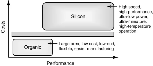
Figure 1.3 provides a conceptual view of the cost-and-performance sectors served by silicon technology and organic semiconductor technology. It must be noted that organic semiconductor devices do not offer the same electrical performance as silicon devices. While silicon technology is aimed for high-end, high performance, and high processing power electronic products, organic semiconductor technology appeals for lower-end, cost-effective disposable electronics products.
Figure 1.3 Illustration of cost versus performance comparison of silicon technology and organic semiconductor technology.
One of the most frequently discussed opportunities for organic electronics is their integration as the driver backplane of flexible displays. Specifically, printed organic semiconductor materials are strong candidates for novel electrically active display media. The same applies to radio frequency interrogation devices. An overview of these OTFT-based applications and their current market status is presented next. Note that, at present, a-Si thin film transistors (TFTs) and polycrystalline silicon (poly-Si) TFTs are the key backplane technologies used in flat panel display products. Therefore, OTFTs are not intended to displace a-Si TFTs in large-area high-resolution flat panel displays. Instead, they will have a bigger impact on lower-cost flexible displays and e-paper applications. The key features of OTFT and a-Si TFT are compared in Table 1.1.
Table 1.1 Comparison of OTFTs and amorphous silicon (a-Si) TFTs
| OTFT | a-Si TFT | |
| Material | Organic semiconductor as active layer; p-type, n-type, ambipolar | a-Si as active layer n-type |
| Processing | Spin-coat, print, evaporation. Low temperature (e.g., room temperature) | Plasma enhanced chemical vapor deposition (PECVD)T < 350 °C |
| Mobility | Can be comparable to a-Si | ∼1 cm2 V−1 s−1 |
| Substrate and form factor | Variety of substrates and flexible form factor | Glass (most common), Plastic (in development) |
| Mechanically flexible | ||
| Mechanical flexibility | Bendable | Fragile and brittle |
| Electrical stability | Rapid degradation, but degradation stabilizes (may be favorable for devices that turn on for a longer time) | Slower bias-induced degradation, but degradation does not stabilize |
| Pros | Potentially no clean-room, lower cost | More mature and stable |
| Cons | Process challenge; device performance, stability, and lifetime | Mechanical flexibility (stress)Higher processing temperature |
| Key applications | Numerous: displays, RFID tags, sensors, disposable electronics | Circuits for large-area displays and sensors array backplane |
| Outlook | New opportunities: smaller/flexible displays, disposable electronics, smart textiles | Continue to excel in AMLCD, AMOLED, active-matrix sensor technologies |
1.1.1 Large-Area Displays
The application of OTFTs for large area displays has been demonstrated by a number of companies and research institutions. For example, Plastic Logic Ltd. demonstrated the integration of an OTFT-driven backplane to a Gyricon display in 2003 [27]. The active-matrix display backplane was inkjet printed and drove a 3000-pixel display that was fabricated on glass. In early 2007, the world's first factory was built to produce plastic electronic devices [18].
A number of corporations have also invested in R&D for OTFT-driven large area displays. Examples include Sony, Samsung, Kodak, LG Philips, Motorola, 3M, and Hewlett-Packard. In 2007, Sony demonstrated a 2.5 in. AMOLED display driven by OTFTs [28]; LG Philips' LCD Division presented a high resolution active-matrix liquid crystal display (AMLCD) with an OTFT-driven backplane fabricated using solution processing [29]; and Samsung Electronics reported an active-matrix display using printed OTFTs [30].
1.1.2 Rollable Displays
The mechanical flexibility of organic materials makes them particularly attractive for rollable or flexible displays. Polymer Vision, a spin off from Royal Philips Electronics, was a pioneer in demonstrating the capability of rollable displays, which were produced by combining ultrathin flexible OTFT-driven active-matrix backplane technology and flexible electronic ink (E-Ink) display technology. In January 2008, Polymer Vision introduced their first rollable display product, called Readius®, a pocket-sized device, combining a 5″ rollable display with high speed connectivity. The Readius® demonstrated a merger of the reading-friendly strengths of electronic-readers with the high mobility features of mobile phones, along with instant access to personalized news and information [31]. Demand for larger mobile displays is accelerating as telecom players push mobile content and mobile advertisements. The solution is to unroll the display when needed and simply store it away when not in use. Therefore, rollable display enabled devices are expected to be an emerging commodity for new generations of portable communication devices, thus presenting exciting commercial opportunities for ...
Table of contents
- Cover
- About the Authors
- Title Page
- Copyright
- Dedication
- Preface
- Glossary
- Chapter 1: Introduction
- Chapter 2: Organic Thin Film Transistor (OTFT) Overview
- Chapter 3: OTFT Integration Strategies
- Chapter 4: Gate Dielectrics by Plasma Enhanced Chemical Vapor Deposition (PECVD)
- Chapter 5: Dielectric Interface Engineering
- Chapter 6: Contact Interface Engineering
- Chapter 7: OTFT Circuits and Systems
- Chapter 8: Outlook and Future Challenges
- Index
Frequently asked questions
Yes, you can cancel anytime from the Subscription tab in your account settings on the Perlego website. Your subscription will stay active until the end of your current billing period. Learn how to cancel your subscription
No, books cannot be downloaded as external files, such as PDFs, for use outside of Perlego. However, you can download books within the Perlego app for offline reading on mobile or tablet. Learn how to download books offline
Perlego offers two plans: Essential and Complete
- Essential is ideal for learners and professionals who enjoy exploring a wide range of subjects. Access the Essential Library with 800,000+ trusted titles and best-sellers across business, personal growth, and the humanities. Includes unlimited reading time and Standard Read Aloud voice.
- Complete: Perfect for advanced learners and researchers needing full, unrestricted access. Unlock 1.5M+ books across hundreds of subjects, including academic and specialized titles. The Complete Plan also includes advanced features like Premium Read Aloud and Research Assistant.
We are an online textbook subscription service, where you can get access to an entire online library for less than the price of a single book per month. With over 1.5 million books across 990+ topics, we’ve got you covered! Learn about our mission
Look out for the read-aloud symbol on your next book to see if you can listen to it. The read-aloud tool reads text aloud for you, highlighting the text as it is being read. You can pause it, speed it up and slow it down. Learn more about Read Aloud
Yes! You can use the Perlego app on both iOS and Android devices to read anytime, anywhere — even offline. Perfect for commutes or when you’re on the go.
Please note we cannot support devices running on iOS 13 and Android 7 or earlier. Learn more about using the app
Please note we cannot support devices running on iOS 13 and Android 7 or earlier. Learn more about using the app
Yes, you can access Organic Thin Film Transistor Integration by Flora Li,Arokia Nathan,Yiliang Wu,Beng S. Ong in PDF and/or ePUB format, as well as other popular books in Technology & Engineering & Electrical Engineering & Telecommunications. We have over 1.5 million books available in our catalogue for you to explore.