- English
- ePUB (mobile friendly)
- Available on iOS & Android
eBook - ePub
Atom Chips
About this book
This stimulating discussion of a rapidly developing field is divided into two parts. The first features tutorials in textbook style providing self-contained introductions to the various areas relevant to atom chip research.
Part II contains research reviews that provide an integrated account of the current state in an active area of research where atom chips are employed, and explore possible routes of future progress. Depending on the subject, the length of the review and the relative weight of the 'review' and 'outlook' parts vary, since the authors include their own personal view and style in their accounts.
Part II contains research reviews that provide an integrated account of the current state in an active area of research where atom chips are employed, and explore possible routes of future progress. Depending on the subject, the length of the review and the relative weight of the 'review' and 'outlook' parts vary, since the authors include their own personal view and style in their accounts.
Trusted by 375,005 students
Access to over 1 million titles for a fair monthly price.
Study more efficiently using our study tools.
Information
PART ONE
FUNDAMENTALS
1
FROM MAGNETIC MIRRORS TO ATOM CHIPS1)
1.1 Introduction
Following the advent of laser cooling and trapping techniques in the 1980s, a new exciting area of research, ‘atom chips’, has emerged in which sophisticated micron-scale structures on planar substrates are produced utilizing the latest technological developments in lithography and nanofabrication. These complex microstructures produce tiny magnetic field configurations which can trap, cool, and manipulate ensembles of ultra-cold atoms in the vicinity of a surface. Scaling down the dimensions of atom trapping geometry offers extended possibilities for the production and control of Bose–Einstein condensates (BECs). Enormous progress on the generation of BECs and quantum degenerate Fermi gases, on-chip matter–wave interferometers, and integrated detectors has been made in the last few years.
In the second section of this article we trace the historical evolution of this new field, from the first surface-based atom optical elements – magnetic mirrors – to the present-day micro-fabricated structures on a substrate – atom chips. In Section 1.3 we present the basic principles of magnetic mirrors for cold atoms and describe different types of magnetic mirror. Section 1.4 describes the production of a BEC on a permanent magnetic film atom chip; the application of this atom chip to probe the topology of magnetic fields using RF spectroscopy and to study the adiabatic splitting of a BEC in a double well for sensing asymmetric potentials; and investigations of the spatially dependent relative phase evolution of a two-component BEC. Finally, in Section 1.5 we describe a permanent magnetic lattice on an atom chip for trapping and manipulating multiple arrays of ultra-cold atoms and quantum degenerate gases.
1.2 Historical Background
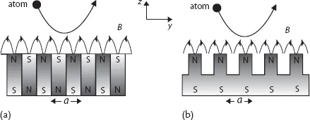
In 1983 Opat [1] proposed the idea of using periodic arrays of electric fields on a planar substrate to reflect beams of polar molecules in a matter–wave interferometer. Almost a decade later the Melbourne group [2] reported the reflection of a beam of chloromethane (CH3Cl) molecules from the exponentially decaying electric field above a periodic array of electrodes of alternating polarity.2) Opat and coworkers [3] then extended these ideas to periodic arrays of magnetic fields to create a surface-based mirror for reflecting beams of laser-cooled atoms (Figure 1.1a). As slowly moving atoms in positive (or ‘low-field seeking’) magnetic states approach the periodic magnetic structure they experience an exponentially increasing magnetic field, with decay length a/2π (where a is the period), and for sufficiently large magnetic fields the atoms are repelled by the structure. A number of schemes [3] were proposed for producing the periodic magnetic structures, including the use of arrays of magnets of alternating polarity, periodic magnetic fields ‘recorded’ on ferromagnetic substrates as in sound recording, and planar arrays of parallel wires alternately carrying electric current in opposite directions. Methods for fabricating the surface-based microstructures were suggested including lithographical techniques used in the electronics industry.
Figure 1.1 Schematic diagram of (a) a magnetic mirror consisting of perpendicularly magnetized elements of alternating polarity, (b) a grooved perpendicularly magnetized microstructure [10].
The first magnetic mirror for cold atoms was realized in 1995 by Roach et al. [4] by recording sinusoidal signals onto a magnetic audio-tape and observing the retroflection of laser-cooled rubidium atoms from the recorded structure. Soon after, Sidorov et al. [5] in Melbourne reported the retroreflection of cold cesium atoms from a 2-mm-period planar array of Nd-Fe-B magnets of alternating polarity. In 1997 the Sussex group demonstrated the focusing and multiple reflection of cold atoms bouncing on a curved magnetic mirror made from a concave-shaped floppy disk or video tape [6, 7].
One of the major challenges was to be able to scale the magnetic structures down to micron-scale periods, in order to produce a hard mirror with very short decay length and minimal finite-size effects. This problem was basically solved when it was shown [8] that a grooved periodic magnetic structure produces a magnetic field distribution that is essentially the same as that above an array of magnets of alternating polarity. The Melbourne group subsequently demonstrated the specular reflection of cold atoms from a 1-μm-period magnetic mirror constructed from micro-fabricated grooved structures coated with perpendicularly magnetized film [9, 10]. The scaling down of the period to 1 μm represented a significant advance in the miniaturization of surface-based atom optical elements.
In 1999 the Melbourne [11] and Harvard/Orsay/Gaithersburg [12] groups reported a magnetic mirror for cold atoms constructed from a planar array of current-carrying conductors lithographically patterned on a silicon wafer or a sapphire substrate. A feature of this type of magnetic mirror is that the magnetic field may be readily varied, switched or modulated by varying the current in the conductors. Such magnetic mirrors were the first micro-fabricated surface-based optical elements for cold atoms and represented a significant step towards the development of more sophisticated atom chips based on micro-fabricated current-carrying conductors on a substrate [13–15].
In an earlier paper, Weinstein and Libbrecht [16] at CalTech had proposed various planar current-carrying wire geometries for constructing microscopic electromagnetic traps for cold atoms including the use of superconducting wire structures. In 1998 Vuletić et al. [17] and Fortágh et al. [18] in Munich demonstrated 3D microtraps for cold atoms based on a combination of electromagnets and permanent magnets or current-carrying conductors, and Drndic et al. [19] at Harvard reported the fabrication of micro-electromagnetic traps with geometries proposed in [16]. In 1999 the Munich group [20] reported the use of surface magnetic microtraps based on a ‘U’-shaped wire quadrupole microtrap and a ‘Z’-shaped wire Ioffe–Pritchard (IP) microtrap, with non-zero potential minimum to eliminate spin-flip losses, for the trapping of cold atoms on a substrate. Soon after, other groups [21–24] demonstrated the guiding of laser-cooled atoms by current-carrying wires, and Davis [25] proposed the use of permanent magnetic structures as miniature waveguides to transport cold atoms on a substrate. In 2000 the Innsbruck group [26] reported the trapping and guiding of cold atoms using a micro-fabricated circuit on a substrate, which they called an ‘atom chip’. In the following year the Munich group [27] demonstrated a magnetic conveyer belt for transporting and merging cold atoms on an atom chip.
A major breakthrough came at the International Conference on Laser Spectroscopy in Snowbird in 2001 when Hänsel et al. [28] from Munich and Ott et al. [29] from Tübingen simultaneously announced the realization of a Bose–Einstein condensate (BEC) of 87Rb atoms in a current-carrying magnetic microtrap on an atom chip. The use of miniature magnetic microtraps allowed the scaling down of the electric currents required to produce a BEC and the scaling up of the trap confinement and elastic collision rate, thus greatly simplifying and speeding up the production of a BEC. In 2006 Aubin et al. ([30], Chapter 12) in Toronto realized a degenerate Fermi gas of 40K atoms on an atom chip by sympathetic cooling with ultra-cold 87Rb atoms.
One of the next big challenges was to see if it was possible to perform coherence or interference experiments on ultra-cold atoms trapped on an atom chip at distances close to the surface (Chapters 4 and 5). In 2004 Treutlein et al. [31] in Munich reported the coherent manipulation of two hyperfine states of ultra-cold 87Rb atoms in a current-carrying magnetic microtrap, with coherence times exceeding 1 s. This opened the way for Ramsey interferometry and miniature atomic clocks on an atom chip ([32], Chapter 8). However, on-chip interferometry by spatially splitting the condensate proved to be more challenging owing to difficulties of phase preservation and control of the condensate. In 2005 the MIT/Harvard groups [33] dynamically split a condensate by deforming a single-well magnetic trap into a double-well potential, but non-adiabatic evolution in a quartic potential during the splitting process led to an unpredictable relative phase. A major breakthrough came when the Heidelberg/Vienna group demonstrated a phase-preserving splitting scheme based on RF-induced adiabatic potentials ([34], Chapter 7), which allowed accurate control over the splitting process and the observation of reproducible interference fringes with a deterministic phase. In the same year the Boulder/Harvard groups [35] achieved splitting, reflection, and recombining of condensate atoms in a Michelson interferometer using a standing-wave light field in a waveguide on a chip. In 2007 the MIT/Harvard groups [36] reported the observation of phase coherence between two separated BECs on an atom chip for times up to about 200 ms after splitting the condensate. In 2009 the Munich group [37] demonstrated the coherent manipulation of BECs in a state-dependent potential with microwave fields on an atom chip, allowing the on-chip generation of multi-particle entanglement and quantum-enhanced metrology with spin-squeezed states [38] (Chapter 8).
Very recently, Deutsch et al. [39] in Paris have reported coherence times as long as 58 s in a Ramsey interferometer experiment on 87Rb atoms trapped on an atom chip. The long coherence times are interpreted in terms of a spin self-rephasing mechanism induced by an identical spin rotation effect that occurs during collisons in the forward direction between two identical particles [40]
In parallel developments Sinclair et al. [41] in London produced a BEC on a permanent-magnet atom chip based on periodically magnetized videotape and Hall et al. [42, 43] in Melbourne produced a BEC in a microtrap on a TbGdFeCo permanent magnetic film atom chip. BECs have since been produced in microtraps on a Co-Cr-Pt hard disk [44] and on a Fe-Pt magnetic foil atom chip [45]. In 2007 Whitlock et al. in Amsterdam [46, 47] constructed a 2D asymmetric magnetic lattice with periods of 22 and 36 μm in orthogonal directions on a Fe-Pt film atom chip and the Melbourne group [48, 49] constructed a 1D 10-μm-period magnetic lattice on a TbGdFeCo film atom chip. Both groups demonstrated the loading of ultra-cold atoms into multiple sites of the permanent magnetic lattice. Magnetic lattices can be readily scaled to have a very large number of lattice sites and could form the basis of storage registers for quantum information processing.
Superconducting wires offer the prospect of an extremely low noise environment for trapped ultra-cold atoms. In 2006 Nirrengarten et al. ([50] and Chapter 10) in Paris reported the trapping of ultra-cold atoms on a superconducting atom chip and the following year Mukai et al. [51] in Tokyo demonstrated the trapping of atoms on a persistent supercurrent atom chip. In 2008 the Paris group [52] realized a BEC on a superconducting atom chip and the Tübingen group [53] demonstrated the Meissner effect using ultra-cold atoms trapped by a superconducting wire on an atom chip. The development...
Table of contents
- Cover
- Related Titles
- Title
- Copyright
- Preface
- List of Contributors
- PART ONE: FUNDAMENTALS
- PART TWO: ULTRACOLD ATOMS NEAR A SURFACE
- PART THREE: COHERENCE ON ATOM CHIPS
- PART FOUR: NEW DIRECTIONS
- Index
Frequently asked questions
Yes, you can cancel anytime from the Subscription tab in your account settings on the Perlego website. Your subscription will stay active until the end of your current billing period. Learn how to cancel your subscription
No, books cannot be downloaded as external files, such as PDFs, for use outside of Perlego. However, you can download books within the Perlego app for offline reading on mobile or tablet. Learn how to download books offline
Perlego offers two plans: Essential and Complete
- Essential is ideal for learners and professionals who enjoy exploring a wide range of subjects. Access the Essential Library with 800,000+ trusted titles and best-sellers across business, personal growth, and the humanities. Includes unlimited reading time and Standard Read Aloud voice.
- Complete: Perfect for advanced learners and researchers needing full, unrestricted access. Unlock 1.4M+ books across hundreds of subjects, including academic and specialized titles. The Complete Plan also includes advanced features like Premium Read Aloud and Research Assistant.
We are an online textbook subscription service, where you can get access to an entire online library for less than the price of a single book per month. With over 1 million books across 990+ topics, we’ve got you covered! Learn about our mission
Look out for the read-aloud symbol on your next book to see if you can listen to it. The read-aloud tool reads text aloud for you, highlighting the text as it is being read. You can pause it, speed it up and slow it down. Learn more about Read Aloud
Yes! You can use the Perlego app on both iOS and Android devices to read anytime, anywhere — even offline. Perfect for commutes or when you’re on the go.
Please note we cannot support devices running on iOS 13 and Android 7 or earlier. Learn more about using the app
Please note we cannot support devices running on iOS 13 and Android 7 or earlier. Learn more about using the app
Yes, you can access Atom Chips by Jakob Reichel, Vladan Vuletic, Jakob Reichel,Vladan Vuletic in PDF and/or ePUB format, as well as other popular books in Physical Sciences & Optics & Light. We have over one million books available in our catalogue for you to explore.