![]()
Chapter 1
Introduction to Communication System-on-Chip, RF Analog Front-End, OFDM Modulation, and Performance Metrics
1.1 Communication System-on-Chip
1.1.1 Introduction
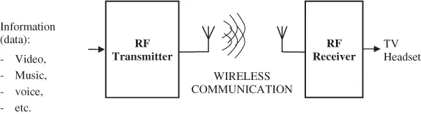
Radio frequency (RF) communication systems use RFs to transmit and receive information such as voice and music with FM, or video with TV, and so on (Steele, 1995; Rappaport, 1996; Haykin, 2001). From a general point of view RF communication is simply composed of an RF transmitter sending the information and an RF receiver recovering the information (Figure 1.1). Below are basic definitions of the vocabulary commonly used in communication systems:
- Signal: Information (data, image, music, voice, …) we want to transmit and receive.
- Carrier frequency: RF sinusoidal waveform, called a carrier because it is used to “carry” the signal from the transmitter to the receiver.
- MODulation: Modifying the carrier waveform in order to convey the information (signal) in transmission.
- DEModulation: Extracting the signal (i.e., the information) from the carrier frequency in reception.
- Antenna: Device which transforms the electrical signal into electromagnetic waves for radiation and vice versa.
- Channel bandwidth: Span of frequencies used for the communication.
- MODEM = MODulator + DEModulator.
- TRANSCEIVER = TRANSmitter + reCEIVER.
In the last decades telecommunications have migrated toward digital technology (Proakis, 1995) as a result of the evolution of advanced digital signal processing (DSP) techniques which can now be deployed at low-cost in mobile devices. Nowadays a mobile phone is not only used for traditional voice calls but as a multimedia platform for surfing the Internet, listening to music, data transfers, localization (global positioning system (GPS)), and so on: many applications which require the implementation of different technologies and communication standards (WiFi, Bluetooth, GSM/3G/4G Long Term Evolution (LTE), GPS, near-field communication (NFC), etc.) on the same platform. Since the phone's form factor and battery life are limited, state-of-the-art integrated circuit (IC) design and system-on-chip (SoC) implementations have become necessities for providing cost-effective solutions to the market.
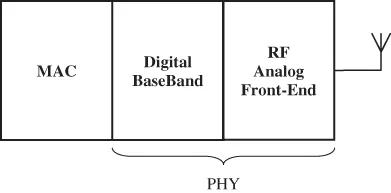
Modern digital communications transceivers (Figure 1.2) are generally composed of a Medium Access Control (MAC) layer managing the access to the medium between different users in a network and the quality of service seen by each, and a PHY (Physical Layer) which is responsible for the transfer of information across the medium (wireless channel, cable, optical fiber, etc.). The PHY can be decomposed into two blocks:
- The digital baseband (DBB) which is located between the MAC and the analog front-end (AFE). The baseband transmission path encodes the bits provided by the MAC, generates the data symbols to be sent across the medium, and finally performs the digital modulation. The reception path demodulates the data and provides a decoded bit stream to the MAC. Generally, the transmission requirements are well specified by the standards (channel coding, modulation, etc.), whereas the algorithms used in reception (channel estimation/equalization, synchronization, etc.) can vary from one implementation to another.
- The RF AFE is connected to the DBB. The RF transmit path converts the DBB signal to analog and frequency up-converts to RF. The receiver frequency down-converts the RF signal to baseband, filters out any interferers, and finally converts the signal to DBB.
1.1.2 CMOS Technology
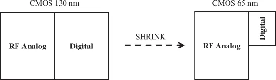
As complementary metal oxide semiconductor (CMOS) technology presents remarkable shrinking properties and cost attractiveness, it has become the unavoidable choice for semiconductors implementing SoC and for low-cost combo-chips integrating several systems on the same die (Abidi, 2000; Brandolini et al., 2005). Although CMOS was initially dedicated to digital design, today RF AFEs are embedded using this technology as well in order to improve the integration efficiency and thus lower the platform cost (Lee, 1998; Razavi, 1998a,b; Iwai, 2000). Nevertheless, CMOS is not well-optimized for RF analog design due to the low ohmic substrate limiting the analog/digital isolation, the low-voltage supply limiting the dynamic range/linearity, and the poor quality factor of the passive components. Furthermore, in deep-submicrometer CMOS technology (nanometer), whereas the digital part of the chip naturally shrinks with the process ratio, the RF analog part scales poorly (Figure 1.3), at around 10% per process node, and generally requires a redesign in order to be able to reduce its area and power consumption. Consequently, for SoC integration the RF AFE remains the major bottleneck in reducing the CMOS transceiver size, therefore requiring more work.
1.1.3 Coexistence Issues
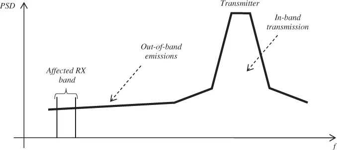
Due to the integration constraints imposed by multi-communication applications, several communication systems often have to coexist on the same platform (such as mobile phone), and in the worst case even on the same chip. Even if the radios do not operate in the same band, any RF transmitter generates broadband out-of-band emissions which can degrade the sensitivity of neighboring receiver bands, as illustrated in Figure 1.4.
If the systems are located on the same platform but not on the same chip, a coupling between antennas, or between chips at the pin level, can occur, as depicted in Figure 1.5. Board design and layout, as well as the distance between the antennas and their orientation, have to be carefully t...