This monograph for young researchers and professionals looking for a comprehensive reference offers an advanced treatment of the topic that extends beyond an introductory work. As such, it systematically covers the inorganic nanostructures in the breadth needed, while presenting them together with the surface science tools used to characterize them, such as electron spectroscopy and scanning probe techniques. The unique challenges in the fabrication of nanostructures are illustrated, and set into context of controlling structure, dimensionality and electronic properties.
Trusted by 375,005 students
Access to over 1.5 million titles for a fair monthly price.
This first chapter can be seen as a warm-up: it will prepare our mental muscles to think about nanomaterials, and why they can be considered as a class of materials in their own right. We will introduce the concept of confinement and dimensionality and derive the density of states (DOS) for low-dimensional structures. After a discussion of electronic properties we will move on to a quite different area of research, and discuss fundamental processes at surfaces, which are rarely included in materials science or physics core classes, but are important for the understanding of many aspects of nanomaterial synthesis.
1.1 Size, Dimensionality, and Confinement
The nanosize regime is defined by the transition between the bulk and atom, and is characterized by a rapid change in material properties with size. Each set of properties (mechanical properties, geometric and electronic structure, magnetic and optical properties, and reactivity) is defined by characteristic length scales. If the size of the system approaches a characteristic length scale, the property in question will be modified dramatically as a function of size. The intimate link between size and material properties is one of the most intriguing aspects of nanoscience, and is at the core of the discipline. The control of size is therefore often the most important, and difficult, challenge in the synthesis of nanostructures.
The decrease in size of a nanostructure is accompanied by a rapid change in the volume-to-surface ratio of atoms: a cube with a side length of 1 mm contains about 2.5·1019 atoms, and the percentage of surface atoms is only 2·10−6; for a cube side length of 1 μm the percentage of surface atoms increases to 2·10−3; and for 1 nm side length, only one true volume atom remains, which is surrounded on all sides by other atoms. This shift from a volume–atom dominated structure, where the majority of atoms has fully saturated bonds, to a surface–atom dominated structure has rather dramatic consequences.
One of the best-known examples, which illustrates the impact of the change in the ratio of surface-to-volume atoms, is the observation of the reactivity of nanosize catalyst particles [1–3]. Catalysts are industrial materials, which are produced in very high volumes and used in nearly every chemical process. The role of a catalyst in a chemical reaction is to lower the activation energies in one or several of the reaction steps, and it can therefore increase yield, reaction speed, and selectivity. Most catalysts contain a relatively high percentage of expensive noble metals, and increasing catalyst efficiency through reduction of its size can thus greatly diminish costs, and at the same time very often boosts efficiency. The reactivity increase with decreasing particle size can be attributed to several size dependent factors: a proportional increase in the number of reactive surface atoms and sites, changes in the electronic structure, and differences in the geometric structure and curvature of the surface, which presents a larger concentration of highly active edge and kink sites. The underlying mechanism of a catalytic reaction is often complex, and cannot be attributed to a single factor such as larger surface area or modulation of the electronic structure. The study of catalysts and catalytic reactions is a highly active field of research, and depends on the improved comprehension of nanoparticle synthesis and properties.
An important step in classifying the functionality of nanostructures is to understand the relation between dimensionality and confinement. Dimensionality is mathematically defined by the minimum number of coordinates required to define each point within a unit; this is equivalent to vectors which define a set of n unit vectors required to reach each point within an n-dimensional space. When looking at nanostructures, the definition of dimensionality becomes more ambiguous: for example, a semiconductor nanowire can have a diameter of a few to several ten nanometers, with a length up to several micrometers. It is a structure with a very high aspect ratio, but in order to describe the position of each atom or unit cell within the wire, a three-dimensional (3D) coordinate system is required with one axis along the wire and the other two unit vectors to describe the position within the horizontal plane. This coordinate system bears no relation to the crystal structure and only serves to illustrate the mathematical dimension of the nanowire. A one-dimensional (1D) nanowire is therefore strictly speaking only present if its thickness is only a single atom. Examples for this kind of 1D system are given in Chapter 3.
The most important aspect for our discussion of dimensionality is the modulation of the electronic structure as a function of the extension of a nanostructure in the three dimensions of space. It is possible to define potential barriers in a single direction in space, thus confining electrons in one direction, but leaving them unperturbed in the other two directions. This corresponds now to a two-dimensional (2D) nanostructure, a so-called quantum well. Going back to our example of the nanowire: the electronic system of the nanowire (if it is sufficiently small) is confined in the two directions perpendicular to its long axis, but not along the long axis itself, and it is therefore a 1D structure. The dimensionality of a nano structure is defined through the geometry of the confinement potential.
Dimensionality for nanostructures is therefore often defined in a physically meaningful manner by considering the directions of electron confinement. Confinement for electrons is introduced in quantum mechanics by using the particle in a box: the electron wave is confined with in the well, which is defined by infinitely high potential energy barriers. The equivalent treatment can be used for holes. The width of the box then controls the energy spacing between the allowed states, which are obtained from solutions of the Schrödinger equation.
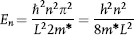
The allowed n-th energy level En is given for a 1D well (a one dimensional box, with only one directional axis) by:
(1.1)
where L is the width of the box, m* is the effective mass of the electron, and n is an integer 1, 2, 3,. . .. This equation emerges directly from the solution of the Schrödinger equation for the free electrons in a 1D box with a width of L, which is described in quantum mechanics textbooks. The energy increases with the inverse of the square of the box size, and n is the corresponding quantum number. This relation is quite general, and specific factors and exponents are modified by the shape of the confinement potential. The highest filled level at a temperature of 0 K corresponds to the Fermi energy (EF) and the quantum well is in its ground state when all levels up to EF are filled. The band gap is the energy difference between the ground state and the first excited state when one electron is excited to the first empty state above EF. If we build a very large quantum well whose dimension approaches that of a macroscopic solid, the energy difference between the ground state and excited state will become infinitesimally small compared with the thermal energy, and the band gap created by quantum confinement for small L disappears; we now have a quasi-continuum of states. The height of the well barrier for a solid is given by the work function of the limiting surfaces.
The band gap in a macroscopic solid forms due to the periodicity of the lattice, which imposes boundary conditions on the electron waves and leads for certain energies to standing waves within the lattice. The standing waves whose wavelengths correspond to multiples of interatomic distances in a given lattice direction define the band gap within the band structure (E(
)) of the material (we are neglecting any structure factors on this discussion). The ion cores define the position of the nodes, and extrema of a standing wave. If the wave vector
satisfies the Laue diffraction condition within the reciprocal lattice, we will observe opening of a band gap at this specific value of
, which is the Brillouin zone boundary. The energy gap opens due to the energetic difference between a wave where the nodes are positioned at the ion cores, and a wave of the same wavelength (wave vector) but where the nodes are positioned in between the ion cores. This argument follows the so-called Ziman model and is described in detail in many textbooks on solid state physics. A semicondcutor or insulator results if the Fermi energy EF is positioned within this bandgap, in all other cases when EF is positioned in the continuum of states, we will have a metal.
If we now start with a metal, where EF lies within the continuum of states, and reduce the size of the system to the nanoscale, which is equivalent to the reduction in the size of the box or quantum well L, the energy difference between states will increase and we can open a band gap for sufficiently small dimensions. The macroscopic metal can become a nanoscopic insulator. For a semiconductor, where a fundamental gap is already present, the magnitude of the gap will increase as confinement drives the increase in separation of the energy levels. The measurement of the magnitude of the band gap is therefore a sensitive measure for quantum confinement and is used in all chapters to illustrate and ascertain the presence of confinement.
In the case of a 2D quantum well, if we define the confinement potential along the z axis, the band structure in x, and y will not be perturbed by confinement. Figure 1.1 shows the energy levels in the quantum well in the direction of confinement, z, and illustrates the sub-band formation. The confinement as described in Equation 1.1 only affects the energy levels in the z direction, while the continuum of levels in the x, and y directions is preserved and for the free electron case the dispersion relation is described by a parabola. Each discrete energy level (set of quantum numbers) in the directions of confinement is associated with the energy levels in the other directions; this leads to the formation of sub-bands. This train of thought can be transferred directly to quantum wires, where confinement is in two directions, and quantum dots, where confinement is in all three directions of space and we have a zero-dimensional (0D) electronic structure. Confinement and formation of sub-bands can substantially change the overall band structure, which is discussed for Si nanowires in the context of the blue shift of emission for porous silicon and a transition from an indirect to direct band gap material for small wire diameters [4–6] (see Chapter 4). The size of the gap is a signature of the impact of confinement, and its increase for decreasing size of a nanostructure is illustrated for several types of materials throughout this book. Silicon nanowires and graphene nanoribbons are examples whe...
Table of contents
Cover
Contents
Title
Copyright
Dedication
Preface
Chapter 1: Dimensions and Surfaces – an Introduction
Chapter 2: Experimental Techniques for Nanoscale Materials Analysis
Chapter 3: Semiconductor Nanowires
Chapter 4: Metal Clusters
Chapter 5: Quantum Dots
Chapter 6: Pure Carbon Materials
Chapter 7: A Few Applications of Inorganic Nanostructures
References
Index
Frequently asked questions
Yes, you can cancel anytime from the Subscription tab in your account settings on the Perlego website. Your subscription will stay active until the end of your current billing period. Learn how to cancel your subscription
No, books cannot be downloaded as external files, such as PDFs, for use outside of Perlego. However, you can download books within the Perlego app for offline reading on mobile or tablet. Learn how to download books offline
Perlego offers two plans: Essential and Complete
Essential is ideal for learners and professionals who enjoy exploring a wide range of subjects. Access the Essential Library with 800,000+ trusted titles and best-sellers across business, personal growth, and the humanities. Includes unlimited reading time and Standard Read Aloud voice.
Complete: Perfect for advanced learners and researchers needing full, unrestricted access. Unlock 1.5M+ books across hundreds of subjects, including academic and specialized titles. The Complete Plan also includes advanced features like Premium Read Aloud and Research Assistant.
Both plans are available with monthly, semester, or annual billing cycles.
We are an online textbook subscription service, where you can get access to an entire online library for less than the price of a single book per month. With over 1.5 million books across 990+ topics, we’ve got you covered! Learn about our mission
Look out for the read-aloud symbol on your next book to see if you can listen to it. The read-aloud tool reads text aloud for you, highlighting the text as it is being read. You can pause it, speed it up and slow it down. Learn more about Read Aloud
Yes! You can use the Perlego app on both iOS and Android devices to read anytime, anywhere — even offline. Perfect for commutes or when you’re on the go. Please note we cannot support devices running on iOS 13 and Android 7 or earlier. Learn more about using the app
Yes, you can access Inorganic Nanostructures by Petra Reinke in PDF and/or ePUB format, as well as other popular books in Tecnología e ingeniería & Ciencias de los materiales. We have over 1.5 million books available in our catalogue for you to explore.