![]()
Chapter 1
General Information About Printed Antennas 1
1.1. Physical characteristics
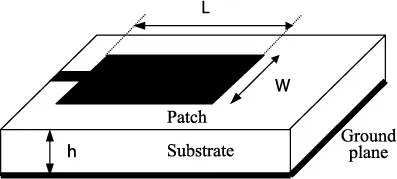
The basic printed antenna consists of a thin layer of metal (patch) positioned over a ground plane, both being etched on the two sides of a substrate of permittivity ε
r and thickness h (
Figure 1.1). Typically, h ≪ λ
0 and 0.003λ
0 < h < 0.05λ
0. The length L of the patch is of the order of
, where ε
eff is the relative permittivity of the patch.
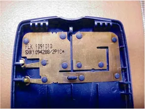
The terms printed, plated, or patch antenna are used interchangeably to describe planar antennas produced using photolithographic techniques. Note that there are planar antennas that are not produced using these techniques. For example, this is the case with PIFA antennas or their variants in 1 GHz mobile telephony, the substrate here being made up of air with metallic parts produced using copper or aluminum foil that has been folded and machined (Figure 1.2).
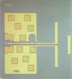
Planar antennas can equally be produced under clean conditions over silicon (Figure 1.3) or glass substrates using microtechnological manufacturing processes. Because of the given antenna dimensions (of the order of 1 cm), the manufacturing costs and patterning tolerances, the applications planned are typically beyond the Ka band (about 20 GHz).
Finally, in very low-cost radio-frequency identification (RFID) applications in which electronic tags are manufactured in bulk, paper or plastic supports are used (Figure 1.4), a conductive ink thereby enabling the production of the radiating element.
Typical permittivity values are in the range 2.2 < εr < 12. Low permittivity and increased substrate thickness lead to superior performance (better efficiency, greater bandwidth, higher directivity) at the cost of a more significant patch width, which can pose problems when antennas are put in an array structure. These dielectric substrate characteristics lead to less concentrated field lines around the patch, which is conducive to radiation.
Inversely, printed microwave circuits require increased permittivity and low substrate thickness to concentrate the field under the metallic sections, to limit the losses from radiation and to minimize the area occupied. There has to be a compromise, therefore, between antenna performance and integration of the feeding circuit, when we want to produce both in the same substrate.
The patch generally takes the form of a square, rectangle, disc, or a horizontal dipole, since these simple geometries lead to good purity of polarization and simple analysis. Printed dipoles possess a wide bandwidth and occupy a reduced space that makes them suitable for use in antenna arrays.
Linear or circular polarizations can easily be produced from all types of patches. Finally, while photolithography enables the simultaneous patterning of the patch array and its distribution circuit, we can easily obtain an increase in directivity, a pattern scanning, or an improvement in purity of polarization, depending on the technique used.
1.2. Properties, limitations, and applications
Printed antennas are of interest in all applications requiring one or more of the following properties:
– low cost;
– mass production, thanks to printed circuit technology;
– planarity;
– lightness;
– consistency on non-planar surfaces (cylinders, etc.);
– mechanical robustness;
properties that we find in wireless communications as well as in embedded systems (aircraft, missiles, etc.). Furthermore, the potential to integrate monolithic microwave integrated circuits (MMICs) or components onto the antenna substrate enables us to envisage:
– miniaturization of the RF front-end receiver;
– reduction in losses in transmission lines;
– reconfiguration capacities in pattern, directivity, polarization, or frequency.
Disadvantages of printed antennas that are often mentioned are:
– poor directivity (from about 6–8 dB);
– reduced efficiency and bandwidth (linked to an increased quality factor Q);
– limited input power;
– reduced purity of polarization;
– radiation interference in power circuits.
However, variants in design or geometry enable a sensible improvement in performance. For example, increasing the thickness of the substrate leads to efficiencies greater than 90% and bandwidths greater than 30%. Stacking patches also enables an increase in bandwidth.
For array applications, planar printed antennas have the following limitations:
– reduced scanning capacity, linked to the zero in the radiation pattern of the radiating element for end-fire directions;
– prohibitive losses in the distribution circuit for antenna arrays of a significant size (approximate directivity > 30 dB);
– significant coupling through surface waves between radiating elements under certain conditions, notably for significant permittivities and substrates of non-negligible thickness, in comparison with the wavelength;
– low maximum power (of the order of 100 W).
Taken from [LUX 07], we summarize below the principle applications of printed antennas and corresponding systems in the area of communications and radar:
– satellites:
- television, direct to homes or vehicles,
- switched arrays for reconfigurable coverage,
- detection of terrestrial resources (synthetic aperture radar imagery),
- antennas for radio-based navigation systems via GPS, Galileo, Glonass (land vehicles or personal assistants and PCs);
– guidance telemetry:
- monopulse systems,
- arrays under radomes;
– adaptive networks:
- multitarget acquisition,
- semiconductor integrated array;
– portable radios or communication with land mobiles:
- mobile telephony (GSM, DCS, PCS, UMTS, etc., portable terminals),
- antennas on base stations,
- FM radio antennas printed on car windscreens,
- toll booths (antennas printed on RF badges);
– aeronautics (aircraft, rocket engines, missiles):
- communication,
- navigation,
- altimeters,
- landing systems,
- antennas conformed onto the fuselage of aeronefs for navigation (radars, altimeters, automatic landing) and communication,
- plated antennas on missiles (telemetry);
– biomedical:
- ...