In-depth overview of two-dimensional semiconductors from theoretical studies, properties to emerging applications!
Two-dimensional (2D) materials have attracted enormous attention due to their exotic properties deriving from their ultrathin dimensions. 2D materials, such as graphene, transition metal dichalcogenides, transition metal oxides, black phosphorus and boron nitride, exhibit versatile optical, electronic, catalytic and mechanical properties, thus can be used in a wide range of applications, including electronics, optoelectronics and optical applications.
Two-Dimensional Semiconductors: Synthesis, Physical Properties and Applications provides an in-depth view of 2D semiconductors from theoretical studies, properties to applications, taking into account the current state of research and development. It introduces various preparation methods and describes in detail the physical properties of 2D semiconductors including 2D alloys and heterostructures. The covered applications include, but are not limited to, field-effect transistors, spintronics, solar cells, photodetectors, light-emitting diode, sensors and bioelectronics.
* Highly topical: 2D materials are a rapidly advancing field that attracts increasing attention
* Concise overview: covers theoretical studies, preparation methods, physical properties, potential applications, the challenges and opportunities
* Application oriented: focuses on 2D semiconductors that can be used in various applications such as field-effect transistors, solar cells, sensors and bioelectronics
* Highly relevant: newcomers as well as experienced researchers in the field of 2D materials will benefit from this book
Two-Dimensional Semiconductors: Synthesis, Physical Properties and Applications is written for materials scientists, semiconductor and solid state physicists, electrical engineers, and readers working in the semiconductor industry.
eBook - ePub
Two-Dimensional Semiconductors
Synthesis, Physical Properties and Applications
- English
- ePUB (mobile friendly)
- Available on iOS & Android
eBook - ePub
Two-Dimensional Semiconductors
Synthesis, Physical Properties and Applications
About this book
Trusted by 375,005 students
Access to over 1.5 million titles for a fair monthly price.
Study more efficiently using our study tools.
Information
1
Introduction
1.1 Background
In 2004, Ander Geim and Konstantin Novoselov from the University of Manchester, UK, first obtained graphene sheets by mechanical exfoliation method, successfully fabricated the first graphene field effect transistor (FET), and investigated its unique physical properties [1]. Before the discovery of graphene, according to the thermodynamic fluctuation law, the two-dimensional (2D) atomic thick layer under nonabsolute zero degrees is unlikely to exist stably [2]. Why is graphene stable at temperatures above absolute zero? Further theoretical studies have shown that this is because large-scale graphene is not distributed in a perfect 2D plane but in a wave-like shape. The experimental results support this view [3, 4]. Therefore, the discovery of graphene shocked the condensed matter physics community and also quickly ignited the enthusiasm of scientists to study 2D materials (a crystalline material composed of a single atomic layer or few atomic layers), indicating the arrival of the “two-dimensional material era.”
In 2010, Ander Geim and Konstantin Novoselov were awarded the Nobel Prize in Physics for their outstanding contribution to graphene (Figure 1.1) [1]. Graphene is a 2D material composed of carbon atoms and having a hexagonal lattice structure. Graphene has good toughness and its Young's modulus can theoretically reach as 1 TPa [5]. Therefore, graphene can form different structures through different curved stacks, such as zero-dimensional fullerenes, one-dimensional carbon nanotubes, and three-dimensional stacked graphite [6].
Graphene has shown many excellent physical properties resulting from the unique structure, and the disappearance of interlayer coupling makes the two carbon atoms in the cell completely equivalent, thus making the effective mass of electrons on the Fermi surface zero [7–11]. Because graphene has a unique Dirac band structure, carriers can completely tunnel in graphene, and electrons and holes in graphene have a very long free path. Therefore, the electronic transport of graphene is hardly affected by phonon collisions and temperature [8]. The mobility of electrons in monolayer graphene is much larger than that in its parent graphite (Figure 1.2c) [16]. In addition, graphene has shown good thermal conductivity (Figure 1.2d) [17], room temperature quantum Hall effect (Figure 1.2a) [12, 14], single-molecule detection (Figure 1.2b), and high light transmission [18]. Graphene is a semimetal material without band gap, it cannot form a good switching ratio in terms of regulation, thus greatly limiting the application of graphene in electronic devices. Although on the bilayer and multilayer graphene, the graphene can obtain a certain band gap by applying an electric field and stress [19]. However, this band gap is not only small but also has a low electrical on/off ratio and is difficult to apply to a controllable device. With the extensive research on two-dimensional materials, it is found that the disadvantages of graphene are compensated for in other families of 2D materials [20–26].

Figure 1.1 Graphene films. (a) Photograph (in normal white light) of a relatively large multilayer graphene flake with thickness ∼3 nm on top of an oxidized Si wafer. (b) Atomic force microscope (AFM) image of 2 μm by 2 μm area of this flake near its edge. Colors: dark brown, SiO2 surface; orange, 3 nm height above the SiO2 surface. (c) AFM image of single-layer graphene. Colors: dark brown, SiO2 surface; brown-red (central area), 0.8 nm height; yellow-brown (bottom left), 1.2 nm; orange (top left), 2.5 nm. Notice the folded part of the film near the bottom, which exhibits a differential height of ∼0.4 nm. (d) SEM micrograph of an experimental device prepared from few-layer graphene, and (e) its schematic view.
Source: Reproduced with permission from Novoselov et al. [1]. Copyright 2004, The American Association for the Advancement of Science.
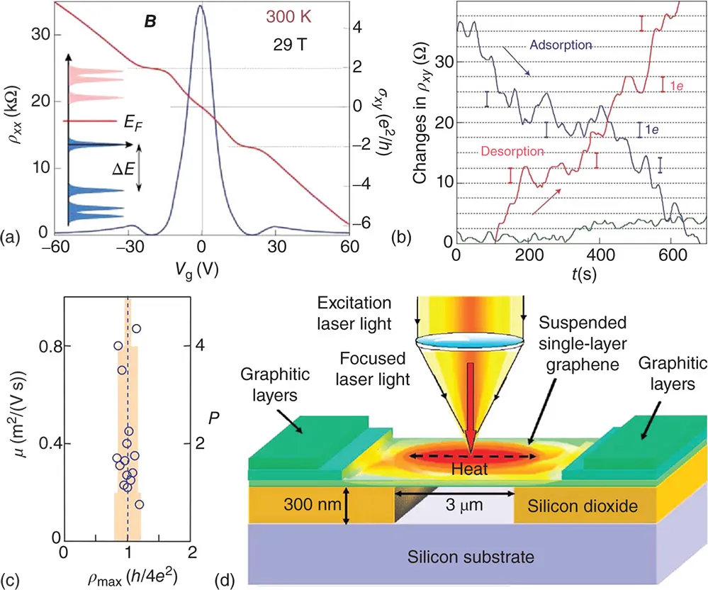
Figure 1.2 (a) Room ...
Table of contents
- Cover
- Table of Contents
- Preface
- About the Authors
- Acknowledgments
- 1 Introduction
- 2 Electronic Structure of 2D Semiconducting Atomic Crystals
- 3 Tuning the Electronic Properties of 2D Materials by Size Control, Strain Engineering, and Electric Field Modulation
- 4 Transport Properties of Two-Dimensional Materials: Theoretical Studies
- 5 Preparation and Properties of 2D Semiconductors
- 6 Properties of 2D Alloying and Doping
- 7 Properties of 2D Heterostructures
- 8 Application in (Opto) Electronics
- 9 Perspective and Outlook
- Index
- End User License Agreement
Frequently asked questions
Yes, you can cancel anytime from the Subscription tab in your account settings on the Perlego website. Your subscription will stay active until the end of your current billing period. Learn how to cancel your subscription
No, books cannot be downloaded as external files, such as PDFs, for use outside of Perlego. However, you can download books within the Perlego app for offline reading on mobile or tablet. Learn how to download books offline
Perlego offers two plans: Essential and Complete
- Essential is ideal for learners and professionals who enjoy exploring a wide range of subjects. Access the Essential Library with 800,000+ trusted titles and best-sellers across business, personal growth, and the humanities. Includes unlimited reading time and Standard Read Aloud voice.
- Complete: Perfect for advanced learners and researchers needing full, unrestricted access. Unlock 1.5M+ books across hundreds of subjects, including academic and specialized titles. The Complete Plan also includes advanced features like Premium Read Aloud and Research Assistant.
We are an online textbook subscription service, where you can get access to an entire online library for less than the price of a single book per month. With over 1.5 million books across 990+ topics, we’ve got you covered! Learn about our mission
Look out for the read-aloud symbol on your next book to see if you can listen to it. The read-aloud tool reads text aloud for you, highlighting the text as it is being read. You can pause it, speed it up and slow it down. Learn more about Read Aloud
Yes! You can use the Perlego app on both iOS and Android devices to read anytime, anywhere — even offline. Perfect for commutes or when you’re on the go.
Please note we cannot support devices running on iOS 13 and Android 7 or earlier. Learn more about using the app
Please note we cannot support devices running on iOS 13 and Android 7 or earlier. Learn more about using the app
Yes, you can access Two-Dimensional Semiconductors by Jingbo Li,Zhongming Wei,Jun Kang in PDF and/or ePUB format, as well as other popular books in Technology & Engineering & Materials Science. We have over 1.5 million books available in our catalogue for you to explore.