Presents technologies and key concepts to produce suitable smart materials and intelligent structures for sensing, information and communication technology, biomedical applications (drug delivery, hyperthermia therapy), self-healing, flexible memories and construction technologies. Novel developments of environmental friendly, cost-effective and scalable production processes are discussed by experts in the field.
eBook - ePub
Carbon-Based Smart Materials
- 194 pages
- English
- ePUB (mobile friendly)
- Available on iOS & Android
eBook - ePub
About this book
Trusted by 375,005 students
Access to over 1.5 million titles for a fair monthly price.
Study more efficiently using our study tools.
Information
1 New class of graphene-based devices for the next generation of nonvolatile memories
Paolo Bondavalli
Thales Research and Technology, Palaiseau Cedex, France
1.1 Introduction
Graphene is a one-atom thick layer of carbon atoms arranged in a hexagonal lattice. Graphene potentialities are attracting a lot of researchers to probe opportunities in a number of directions in the “more Moore” or “beyond CMOS” optics in order to identify the new future technologies [1, 2, 3]. Another promising utilization of graphene and related nanomaterials is to fabricate nonvolatile memories (NVM) exploiting their “memresistive” behavior storing a value of electrical resistance in a permanent way. This happens when a current passing through the materials changes the level of resistance. Therefore, resistive memory exploits the change in the resistance of a material under the effect of an electric field as an information write/erase principle for nonvolatile data storage. The reading of resistance states is nondestructive, and the memory devices can be operated without transistors in every cell [4, 5], as for flash-type memories [6, 7, 8, 9, 10] (see Section 1.2.2), thus achieving a classic cross-bar structure. This kind of memories is called resistive random-access memory (RRAM or ReRAM) and is only one of the possible types of nonvolatile ways to store information in a permanent way. One of the most important advantages of these new classes of 2D materials is that these materials can be implemented in flexible electronics [11, 12, 13, 14, 15], in the form of one-thick atom layers as for graphene or in the form of layers of flakes of graphene oxide (GO) or reduced GO (R-GO), thereby reducing the final cost of the final device exploiting roll-to-roll fabrication [16]. Another great advantage of ReRAMs is their potential to implement them by exploiting only two terminals to work (two contacts and not three as a common transistor, which has drain, source and gate, e.g., flash-type memories), which could dramatically reduce the circuitry and allow to implement easily in 3D architectures by using the roll-to-roll fabrication technique. Potentially, this is applied in various fields such as health monitoring [17, 18, 19, 20, 21], intelligent packaging [22, 23], cards, labels, badges, value paper and medical disposables. Another potential field is the radiofrequency identification (RFID). This is a technology to electronically record the presence of an object using radio signals. Indeed, an innovative alternative pathway to reduce RFID costs and integrate a memory chip to store data is to eliminate the silicon substrate completely, and produce RFID and memory on the same flexible plastic substrate as the antenna [24, 25, 26]. Thanks to graphitic layers, the antenna and chip can be built on the same low-cost substrate, and attachment costs can be removed.
1.2 Graphene-based NVM
As outlined in the International Technology Roadmap for Semiconductors 2011 section concerning Emerging Research Devices, “ultrathin graphite layers are interesting materials for macromolecular memories thanks to the potential fabrication costs that are considered as the primary driver for this type of memory, while extreme scaling is de-emphasized.” The main drawback is related to the fact that memory operation mechanisms and the physics are still unclear and that a deeper research in this field is necessary to improve the comprehension of the phenomenon and the efficiency of the devices. These are not the same physical mechanisms exploited in memories based on graphene-related materials, which will be discussed in the next paragraphs.
1.2.1 Graphene and graphitic layers
The first paper highlighting the utilization of graphene for resistive NVM exploiting two terminal structures was issued in 2008 by Stadley et al. at Caltech [27]. They reported the development of an NVM element based on graphene break junctions. These junctions were obtained by achieving two-terminal devices, transferring graphene sheets on SiO2/Si substrate and depositing metal electrodes on them using e-beam lithography process. After applying a specific voltage under ultravacuum condition (10−7 torr), they were able to create a break in the graphene layer (see Figure 1.1). In these papers, all the measurements were performed under ultravacuum to avoid environmental gas interferences, which strongly reduces the potential utilization of the device.
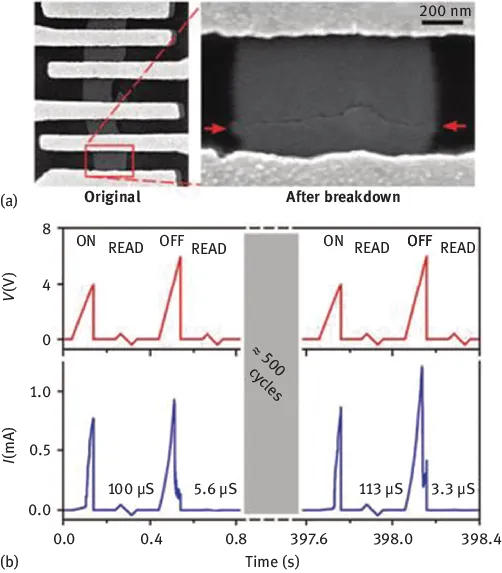
Figure 1.1: (a) SEM image of the device before (left panel) and after breakdown (right panel). The arrows indicate the edges of the break in the graphene layer. (b) Repeatable programming over hundreds of cycles. Upper left panel: Voltage applied to the junction versus time. A ramp with a peak value of ∼4 V corresponds to an ON pulse, while a ramp with a peak value of ∼6 V corresponds to an OFF pulse. A small sawtooth-shaped read-out pulse is applied after each write to determine the junction conductance. Lower left panel: Current flow through the junction, with the low-bias conductance labeled above each read-out pulse. Right panels: Similar data taken after approximately 500 intervening cycles, demonstrating the reproducibility of the switching behavior [27].
After cycling the memories, they observed that the resistance values clearly changed as a function of the voltage (see Figure 1.1b): they moved from a high resistance state (off state) to a lower one as a function of the voltage (on state). This effect was nonvolatile and the devices were cycled thousands of writing cycles (105), showing long retention times (more than 24 h, only limited by measurements).
The reproducibility of the switching behavior was very promising. One of the more coherent explanations was related to the fact that the conductance occurred along a small graphene ribbon that bridges the contacts. To better understand the underlying physical mechanism, researchers studied the time-resolved behavior of the switch from the OFF to ON states, shown in Figure 1.2a. The conductance I/V showed well-defined steps, with magnitude ∼GQ. Here GQ is 2e2/h, the conductance quantum, where e is the electron charge and h is Planck’s constant. Since GQ is the conductance of a spin-degenerate one-dimensional conductor, for example, a linear chain of gold atoms [28], observation of steps in the conductance suggests that the conductance states of a device are likely multiples of highly transmitting quantum channels. Authors proposed a model for device operation based on the formation and breaking of carbon atomic chains that bridge the junctions (see Figure 1.2a, right figure). This mode and the results seem to put in evidence the potential for multiresistive states.
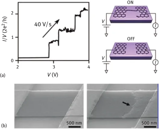
Figure 1.2: (a) Left side: Change in I/V as a function of V pointing out the quantic behavior linked to the formation of atomic chains. Right side: Proposed physical mechanism at the base of the nonvolatile resistive behavior (formation of atomic carbon chains). (b) Tilted-view SEM images of two different devices before and after applying the voltage difference that is necessary to break the layers defined as Vbreak. The arrow shows the fracture across the stripe due to Vbreak [29].
The same physical explanation can be evoked fo...
Table of contents
- Title Page
- Copyright
- Contents
- Preface
- 1 New class of graphene-based devices for the next generation of nonvolatile memories
- 2 Plasma surface activation and functionalization of carbon-based materials
- 3 Modeling carbon-based smart materials
- 4 Carbon nanotube-based materials for space applications
- 5 Molecular dynamics simulations of graphene-based polymer nanocomposites
- 6 Carbon from waste source for Li-ion battery
- Index
Frequently asked questions
Yes, you can cancel anytime from the Subscription tab in your account settings on the Perlego website. Your subscription will stay active until the end of your current billing period. Learn how to cancel your subscription
No, books cannot be downloaded as external files, such as PDFs, for use outside of Perlego. However, you can download books within the Perlego app for offline reading on mobile or tablet. Learn how to download books offline
Perlego offers two plans: Essential and Complete
- Essential is ideal for learners and professionals who enjoy exploring a wide range of subjects. Access the Essential Library with 800,000+ trusted titles and best-sellers across business, personal growth, and the humanities. Includes unlimited reading time and Standard Read Aloud voice.
- Complete: Perfect for advanced learners and researchers needing full, unrestricted access. Unlock 1.5M+ books across hundreds of subjects, including academic and specialized titles. The Complete Plan also includes advanced features like Premium Read Aloud and Research Assistant.
We are an online textbook subscription service, where you can get access to an entire online library for less than the price of a single book per month. With over 1.5 million books across 990+ topics, we’ve got you covered! Learn about our mission
Look out for the read-aloud symbol on your next book to see if you can listen to it. The read-aloud tool reads text aloud for you, highlighting the text as it is being read. You can pause it, speed it up and slow it down. Learn more about Read Aloud
Yes! You can use the Perlego app on both iOS and Android devices to read anytime, anywhere — even offline. Perfect for commutes or when you’re on the go.
Please note we cannot support devices running on iOS 13 and Android 7 or earlier. Learn more about using the app
Please note we cannot support devices running on iOS 13 and Android 7 or earlier. Learn more about using the app
Yes, you can access Carbon-Based Smart Materials by Constantinos A. Charitidis, Elias P. Koumoulos, Dimitrios A. Dragatogiannis, Constantinos A. Charitidis,Elias P. Koumoulos,Dimitrios A. Dragatogiannis in PDF and/or ePUB format, as well as other popular books in Technology & Engineering & Industrial & Technical Chemistry. We have over 1.5 million books available in our catalogue for you to explore.