![]()
1
Mixed-Signal Integrated Systems: Limitations and Challenges
CONTENTS
1.1 Integrated circuit design flow
1.2 Design technique issues
1.3 Integrated system perspectives
1.4 Built-in self-test structures
1.5 Concluding remarks
1.6 To probe further
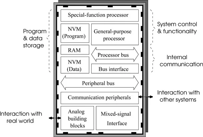
The objective of designing a complete system on a single chip has resulted in the complexity increase of application-specific integrated circuits (ASICs), application-specific standard parts (ASSPs), and very large-scale integrated circuits. The system on a chip (SoC), as shown in Figure 1.1, generally possesses complex signal paths through both analog devices and digital components (nonvolatile memory (NVM), random access memory (RAM), and digital signal processor (DSP)).
FIGURE 1.1
Example of an SoC floorplan.
Examples include multimedia devices, wireless transceivers, sensor and actuator controllers, instrumentation systems, and biomedical devices. The functions, which are realized in the analog domain, include:
☐ Biasing
☐ Sensor and actuator signal conditioning
☐ Driver and buffer
☐ Signal down-conversion and up-conversion
☐ Mixed-signal DSP interfaces
☐ Clock signal generation and frequency synthesis
They are implemented using basic building blocks such as:
• Voltage and current references
• Low-noise and power amplifiers
• Variable-gain amplifier and automatic gain control circuit
• Filter
• Oscillator
• Mixer
• Sample-and-hold circuit
• Analog-to-digital converter
• Digital-to-analog converter
• Phase-locked loop (PLL) and delay-locked loop (DLL)
• Input/output link transceiver
The SoC digital section essentially requires microprocessors, digital signal processors, memories, and control logics. The most important issues are then related to the integration of analog and digital sections. A fully monolithic chip appears to be limited, for instance, by the problematic isolation of analog sections with high-gain bandwidth from the noise generated by the substrate and digital circuits. Furthermore, the device-level simulation of mixed-signal integrated circuits in a realistic environment remains a challenge and testing chips with several complex functions is a difficult task.
1.1 Integrated circuit design flow
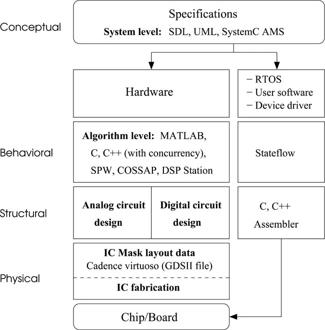
The specification partition into subsystems is illustrated in Figure 1.2. Tools such as SDL (Specification and Description Language), UML (Unified Modeling Language), and SystemC AMS are used to analyze the design at the higher level. At the system level, the design specifications are partitioned into hardware and software components. Note that SystemC AMS is particularly suited to provide functional modeling, architectural exploration, virtual prototyping, and integration validation for analog mixed-signal systems.
FIGURE 1.2
Specification partition into subsystems.
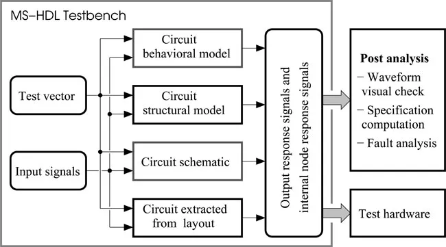
FIGURE 1.3
Circuit design verification.
The development of signal processing algorithms can be performed using MATLAB®, SPW (Signal Processing Workbench), COSSAP (Communication System Simulation and Application Processor), DSP Station, C, and C++ (extended to handle concurrency). To help manage the complexity, the design implementation in hardware is supported by providing a link to hardware synthesis tools.
The functional description is realized by an analog circuit and a digital circuit, which can be designed and verified using various computer-aided design programs such Cadence, Synopsys, and Mentor Graphics tools. When the data processing in the digital domain may require processors or microcontrollers, the design of a real-time operating system (RTOS), application software and device driver is necessary. Besides allowing a modular and scalable programming approach, the desirable features of an RTOS include the ability to provide basic support for task scheduling, resource management, inter-task and input-output communication such that the processor functionality is available to application software in an optimized and predictable way. Stateflow is an interactive design and simulation tool that can be used to describe complex logic, such as an RTOS, in a form that can easily be coded using C/C++ language or assembler.
The functional description can also be refined to analog and digital models, which can be analyzed and verified using a simulator that can interpret mixed-signal hardware description languages (MS-HDLs). Verilog-AMS and VHDL-AMS are two examples in this category (VHDL stands for very highspeed integrated-circuit HDL). MS-HDLs are particularly well suited for the verification of very large and complex mixed-signal integrated circuit designs. An MS-HDL testbench, as shown in Figure 1.3, provides the stimulus required to drive various representations of a circuit while the response signals at nodes of interest are monitored. Specifications are checked by comparing the behavioral and structural models, while the implementation is verified by emphasizing the similarities between the circuit schematic and the circuit extracted from the layout.
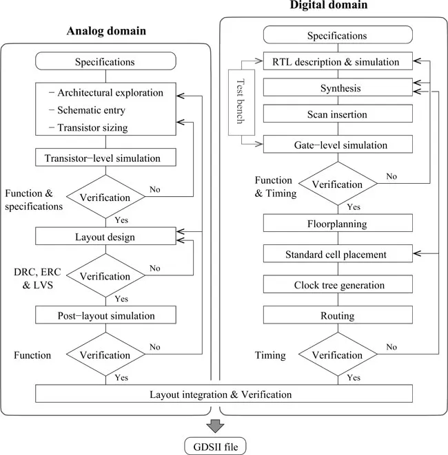
The design flow of an integrated system is illustrated in Figure 1.4. The top-down synthesis process consists of the topology selection, specification translation or circuit sizing, and design verification (design rule check (DRC), electrical rule check (ERC), and layout versus schematic (LVS)). It is then followed by a bottom-up generation and verification of the circuit layout. The performance specifications are required at each step. Throughout the design flow, any change should be taken into account by propagating the associated constraints down the hierarchy, thus ensuring that the top-level block meets the target specifications.
Nowadays, the methodologies of top-down design and bottom-up verification are well-accepted standards in the digital domain. From bit true models of signal processing algorithms, C, Verilog, or VHDL code is generated or written for custom hardware or a DSP-based software solution. By defining a digital circuit at an architectural or behavioral level rather than at the gate level, hardware description languages, such as Verilog or VHDL, can help manage more large designs than tools based on schematic entry. An automated design flow is then adopted to convert the high-level description of the circuit into industry-standard output formats, such as GDSII, that can be integrated into chip layout tools.
In the analog domain, the current design approach — design, simulate, optimize circuit specifications taking into account parasitic effects and process variations, repeat — can be very time consuming for large circuits and relies mostly on designer experience. This is due to the fact that second-order effects in analog circuits are difficult to model as the design evolves and automated tools are actually not available. Furthermore, the use of deep submicrometer CMOS processes contributes to making the verification of analog circuits substantially more difficult, as self-calibration or error cancelation schemes are often required to overcome the limitations of the components, thereby increasing the number of operating modes, behavioral complexity, and size of analog circuits.
FIGURE 1.4
Design flow for an integrated system.
The integration of circuit components takes place either during the physical design phase or after the fabrication. Physical design involves the floor-planning, timing optimization, placement and routing, or layout. The system timing and signal integrity verification is achieved by checking the electrical and design rules and comparing the layout and schematic. Detailed physical design information is required for accurate resistance, inductance, and capacitance parasitic extraction, and delay estimation. Note that the final system should include both hardware and software. The software platform binds the programmable cores and memories via the RTOS, the input-output interface via the device drivers, and the network connection via the communication subsystem.
1.2 Design technique issues
At the system level, an efficient solution is required for managing concurrency or assuring a real-time data flow. This is important for complex chips, which handle multiple tasks at the same time and in cases where the latency due to the interconnect delay dominates the signal bandwidth. The design reuse results in a reduction of the cost and development time. A higher level of abstraction is necessary to create a library of subsystems that can be used for different designs. The design of a complex chip should also include an adequate strategy for the verification of the functional blocks. The logic simulation is a suitable method for the functional verification. Here, the system is tested over a wide variety of operating conditions using simulated input patterns. However, the complexity of the chip can reduce the effectiveness of finding possible design errors. This is related to the higher number of likely events and the difficulty of determining whether the simulated behavior is correct. SoC testing suffers also from the lack of effective coverage metrics, that is, it is not always clear whether enough verification has been completed to confirm the reliability of a chip.
During the design, the circuit optimization is made with respect to timing, power, and area specifications for given values of interconnect load capacitances which can be different from the ones extracted from the final layout, specifically in deep submicrometer technologies. In addition, metal resistance effects are topology dependent and increase with the routing length, and the prediction of the delay propagation is not simple. That is, one-pass synthesis success becomes unlikely due to the requirement of physical design information. A possible solution can consist of using synthesis methods based on the delay equalization of all subsystems and the wire planning among blocks. The speed-power performance of a design based on a submicrometer integrated circuit (IC) process appears to be affected by the substrate and crosstalk-induced noises, signal delay, and parasitic inductance. The coupling effects can be controlled using low-swing differential pair structures, shield wires and repeater insertions, upper and lower bounding slew times, and increased spacing between wires. The increase in functionalities and operating frequencies results in more power dissipation. However, in addition to the supply voltage scaling, power consumption can be reduced by switching off unused subsystems via gated clocking modes.
It can be predicted that the use of an IC process with low geomet...