The manufacture of flash memory, which is the dominant nonvolatile memory technology, is facing severe technical barriers. So much so, that some emerging technologies have been proposed as alternatives to flash memory in the nano-regime. Nonvolatile Memory Design: Magnetic, Resistive, and Phase Changing introduces three promising candidates: phase-change memory, magnetic random access memory, and resistive random access memory. The text illustrates the fundamental storage mechanism of these technologies and examines their differences from flash memory techniques. Based on the latest advances, the authors discuss key design methodologies as well as the various functions and capabilities of the three nonvolatile memory technologies.
- 203 pages
- English
- ePUB (mobile friendly)
- Available on iOS & Android
eBook - ePub
About this book
Trusted by 375,005 students
Access to over 1.5 million titles for a fair monthly price.
Study more efficiently using our study tools.
Information
1
Introduction to Semiconductor Memories
1.1 Classification and Characterization of Semiconductor Memories
Semiconductor memories that can be used to store user data, program code, and other information play an important role in computing systems and embedded systems. A memory system can store millions of words, and each word contains many bits. Because of the rapid development of information technology, the requirements for speed and capacity of the memory system are increasing. Therefore, memory manufacturers and designers need to continuously improve the process technologies and design methodologies in order to enable technology scaling and provide better performance by paying a lower cost.
Based on the functionalities, semiconductor memory can be divided into read-only memory (ROM) and read-write memory, as shown in Figure 1.1. Read/write memory is sometimes called random-access memory (RAM), which is a little confusing because ROM can also be randomly accessed.
The core of a semiconductor memory system is its memory array, shown in Figure 1.2. Here, each storage unit in the array is called a cell. One memory cell can usually store one bit of data. We call this a single-level cell (SLC). Some memory technologies can store more than one bit of data in one memory cell, and this is called a multilevel cell (MLC). A memory array is commonly implemented in the form of square in order to reduce the complexity of the decoder circuitry and to reduce the maximum interconnecting wire length.
In addition to the memory array, address decoders are necessary in order to identify the memory cells to be accessed. Write circuitry and sense amplifiers are respectively used to program the memory cells and read out the stored data. Interface circuits are required to connect the array to external signals. Other circuits, such as control logic, are also required in order to make the memory system function properly.
Currently, the most commonly used semiconductor memories are ROM (including some programmable ROM), static RAM (SRAM), dynamic RAM (DRAM), and nonvolatile memories.
1.1.1 Read-Only Memory
Read-only memory can be simply implemented by using only one transistor per bit as shown in Figure 1.3. Therefore, it can reach very high density compared to other memory structures. In Figure 1.3, the 0/1 of each bit is realized through the absence/presence of an N-channel metal–oxide–semi-conductor field-effect transistor (NMOS) transistor in the corresponding position. When a word line is activated, the absence/presence of an NMOS transistor causes the corresponding isolated/connected bit line to ground. Hence, the different voltages can be generated at bit lines, which are translated to different binary values after amplification by the inverters connected to the bit lines. For example, the content of the ROM in Figure 1.3 is
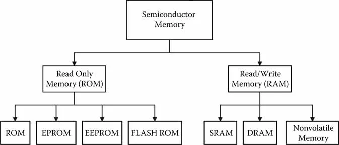
Figure 1.1
Categorization of semiconductor memory.
Categorization of semiconductor memory.
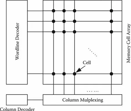
Figure 1.2
Basic memory structure.
Basic memory structure.
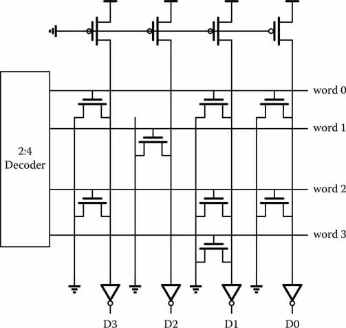
Figure 1.3
Simple ROM structure.
Simple ROM structure.
Word0:1011
Word1:0100
Word2:1011
Word3:0010
Instead of utilizing the absence/presence of transistors to achieve logic 0/1, ROM can also be implemented by the absence/presence of the contact between the metal layer and the gate of each transistor. In other words, a transistor exists in every cell position of the array, but not all of them contact the metal layer and make the connection. This design has a uniform structure and can provide more flexibility: if the content of the ROM needs to be changed, only the contact layer needs to be replaced, without impacting any other layers.
ROM can be used in applications in which the data will be kept permanently unchanged; for example, the lookup table content for some decoders or the program code for a vending machine. The data stored in ROM are nonvolatile, which means that even if we remove the power supply of the memory system, the data inside will not be lost.
The data in ROM are predetermined at the design stage and cannot be changed after fabrication. However, many applications require reprogrammability. For instance, the secret key stored in a smartcard should be nonvolatile. However, each smartcard user needs to own a unique key, which can only be determined postfabrication. In such a situation, ROM is not enough and reprogrammability is essential.
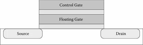
Figure 1.4
Floating gate structure of EPROM.
Floating gate structure of EPROM.
1.1.2 Erasable Programmable ROM and Flash Memory
Erasable programmable ROM (EPROM) is nonvolatile as well as programmable. It uses a special storage cell in order to achieve certain useful characteristics as shown in Figure 1.4. This cell is made of a transistor with two gates. On the top there is a primary gate (or control gate), and an insulated gate, called a floating gate, is placed in the middle. A binary value of an EPROM depends on the threshold voltage of the transistor, which is determined by whether the floating gating charged or not. Because the floating gate is insulated, the electrons within it can be kept from escaping for a long time; that is, more than 10 years.
When programming an EPROM cell, we can apply a high voltage (approximately 25 V) to the control gate. The electrons in the substrate can jump into the floating gate because of a process called avalanche injection, where the electron-hole pairs are generated under high voltage. As a result, the threshold voltage of the transistor can be increased to a level to keep the transistor in “off” mode.
To erase the data, the EPROM has to be exposed to a strong ultraviolet (UV) light from a mercury vapor light source for a certain time until the electrons in the floating gate gain enough energy to escape from it. Accordingly, the chip package of EPROM usually has a small quartz window to admit UV light for erasure. The erase operation can take 20–30 minutes.
This type of EPROM uses the presence/absence of electrons in the floating gate to represent the binary data. One major disadvantage is that the EPROM chip has to be taken out of the system and exposed to UV light when erasure is needed.
1.1.3 Electrically Erasable Programmable ROM
In many applications, it is not realistic to remove the memory chip from the system to erase the stored data. The advent of electrically erasable programmable ROM (EEPROM), which can be programmed and erased within the system by electrical methods, has solved this problem.
The basic storage cell in EEPROM is similar to that in EPROM, as shown in Figure 1.5. There are two gates: the control gate on the top is used for programming/erasing and the floati...
Table of contents
- Cover Page
- Title Page
- Copyright Page
- Contents
- Preface
- Author Biographies
- 1 Introduction to Semiconductor Memories
- 2 Phase Change Memory
- 3 Spin-Transfer Torque RAM
- 4 Resistive Random Access Memory
- 5 Memristors
- 6 The Future of Nonvolatile Memory
- Index
Frequently asked questions
Yes, you can cancel anytime from the Subscription tab in your account settings on the Perlego website. Your subscription will stay active until the end of your current billing period. Learn how to cancel your subscription
No, books cannot be downloaded as external files, such as PDFs, for use outside of Perlego. However, you can download books within the Perlego app for offline reading on mobile or tablet. Learn how to download books offline
Perlego offers two plans: Essential and Complete
- Essential is ideal for learners and professionals who enjoy exploring a wide range of subjects. Access the Essential Library with 800,000+ trusted titles and best-sellers across business, personal growth, and the humanities. Includes unlimited reading time and Standard Read Aloud voice.
- Complete: Perfect for advanced learners and researchers needing full, unrestricted access. Unlock 1.5M+ books across hundreds of subjects, including academic and specialized titles. The Complete Plan also includes advanced features like Premium Read Aloud and Research Assistant.
We are an online textbook subscription service, where you can get access to an entire online library for less than the price of a single book per month. With over 1.5 million books across 990+ topics, we’ve got you covered! Learn about our mission
Look out for the read-aloud symbol on your next book to see if you can listen to it. The read-aloud tool reads text aloud for you, highlighting the text as it is being read. You can pause it, speed it up and slow it down. Learn more about Read Aloud
Yes! You can use the Perlego app on both iOS and Android devices to read anytime, anywhere — even offline. Perfect for commutes or when you’re on the go.
Please note we cannot support devices running on iOS 13 and Android 7 or earlier. Learn more about using the app
Please note we cannot support devices running on iOS 13 and Android 7 or earlier. Learn more about using the app
Yes, you can access Nonvolatile Memory Design by Hai Li,Yiran Chen in PDF and/or ePUB format, as well as other popular books in Technology & Engineering & Computer Engineering. We have over 1.5 million books available in our catalogue for you to explore.