![]()
1
Introduction to Compact Models
1.1 Compact Models for Circuit Simulation
Compact models of a circuit element are simple mathematical descriptions of the behavior of that circuit element, which are used for computer-aided design (CAD) and analysis of integrated circuits (ICs). Compact models describe the device characteristics of a manufacturing technology by a set of physics-based analytical expressions with technology-dependent device model parameters that are solved by a circuit simulator for circuit analysis during IC design. Compact modeling refers to the art of generating compact models of an IC process technology by extracting elemental model parameters for accurate prediction of the behavior of the circuit elements of that technology in circuit simulation. In reality, the complete compact models include the modeling of each circuit element along with its parasitic components that run robustly for realistic assessment of the representative IC technology in circuit CAD [1,2].
Compact models of the circuit elements of an IC manufacturing technology have been the major part of electronic design automation (EDA) tools for circuit CAD since the invention of ICs in the year 1958 [3] and are playing an increasingly important role in the nanometer-scale system-on-chip design era. Today, compact models are the most important part of the process design kit [4,5], which is the interface between circuit designers and device technology. As the mainstream complementary metal-oxide-semiconductor (CMOS) technology is scaled down to the nanometer regime, a truly physical and predictive compact model for circuit CAD that covers geometry, bias, temperature, DC, AC, radio frequency (RF), and noise characteristics has become a major challenge for model developers and circuit designers [1]. A good compact model has to accurately capture all real-device effects and simultaneously produce them in a form suitable for maintaining high computational efficiency.
In the microelectronics industry, compact modeling includes (1) compact device models of the active devices such as bipolar junction transistors (BJTs) and metal-oxide-semiconductor field-effect transistors (MOSFETs) along with the parasitic elements of the active devices; and (2) compact interconnect models of the resistors, capacitors, and inductors of the metallization layers connecting the active devices in the ICs.
1.1.1 Compact Device Models
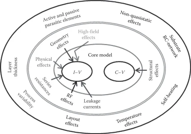
Compact device models describe the terminal behavior of a device in terms of the current-voltage (I–V), capacitance-voltage (C–V), and the carrier transport processes within the device. Figure 1.1 shows the basic features of a typical compact device model of a representative IC technology. As shown in Figure 1.1, a compact model is made of a core model along with the various models to account for the effects of the geometry and physical phenomena in the device. For a metal-oxide-semiconductor (MOS) transistor, the core model describes I–V and C–V behavior of an ideal large MOSFET device [4] of a target technology. The core model represents about 20% of the model code in terms of both execution time and the number of lines in the code. The rest of the model code comprises multiple models that describe the numerous real-device effects that are responsible for the accuracy of the compact model. For MOSFET devices, device phenomena accompanying the core model include short-channel effects (SCEs), output conductance, quantum mechanical effects (QMEs), nonuniform doping effects, gate leakage current, band-to-band tunneling, noise, non-quasistatic (NQS) effect, intrinsic input resistance, and strain effect [4,6].
FIGURE 1.1
A typical composition of compact models of an IC technology: the core model includes the basic I–V and C–V behavior of a large geometry device in the inner circle; the core model is accompanied by the models for physical phenomena within the device and geometry and structural effects as shown in the middle circle; the final compact model with the geometrical and physical effects includes the external phenomena such as ambient temperature, layout effects, process variability, and NQS effects as shown in the outer circle of the model.
The compact model for circuit CAD is the bridge between the circuit design and processing groups and is a module of the extended technology CAD (TCAD) environment [7]. In the extended TCAD environment, the compact model plays an important role in developing next generation IC fabrication technology and assesses the manufacturability of IC fabrication processes by reverse modeling [7,8].
1.1.2 Compact Interconnect Models
Today’s very-large-scale-integrated (VLSI) circuits consist of MOSFET devices and their interconnections, referred to as interconnects. In a typical VLSI chip, the active area is about 10% whereas the physical area is occupied by interconnect and isolation regions 6–10 times the active device area [9]. For this reason, the role of the interconnect is becoming increasingly important as the feature size is scaled down to decananometer regimes and the device density is increased on the chip. As VLSI technology shrinks below 22-nm geometries with Cu/low-k interconnections, parasitics due to interconnections are becoming a limiting factor in determining circuit performance. Therefore, accurate modeling of interconnect parasitic resistance (R), capacitance (C), and inductance (L) is essential in determining various on-chip interconnect-related issues, such as delay, cross talk, energy losses in R due to the current (I) flow or IR drop, and power dissipation. Accurate compact interconnect models are crucial for the design and optimization of advanced VLSI circuits for 22-nm CMOS technology and beyond. In addition, with the emergence of technologies such as carbon nanotubes and graphene nanoribbons, compact interconnection models that are suitable for these technologies are crucial for advanced circuit design. Currently available interconnect models, which are based on field solvers, are inadequate for accurate and meaningful analyses of today’s chips, which house millions of devices. Interconnect models can accurately simulate on-chip global interconnections and speed-power optimization for advanced interconnect technologies. Modeling of these interconnect properties is thus important and must be included by the designer when checking circuit performance in circuit CAD. Though interconnect models are an essential part of optimizing VLSI circuit performance, interconnect modeling is outside the scope of this book; interested readers may refer Saha et al. [10] for recent development of interconnect models. In this treatise, compact modeling of field-effect transistors (FETs) and their parasitic components that are used in the mainstream VLSI circuit design are described.
1.2 Brief History of Compact Device Modeling
Since the 1960s, compact models for circuit CAD have continuously evolved [6]. After the invention of the bipolar transistor in 1947 [11,12], complete circuits including both active and passive devices were realized on monolithic silicon substrates by late 1950s. Computer simulation evolved as a practical way to predict circuit performance including nonlinearities because digital computers were capable of complex circuit analysis based on a network or matrix formulation. The 1950s and 1960s were dominated by BJT technology; the Ebers–Moll (EM) model has been the major large-signal compact model for bipolar transistors since its formulation in 1954 [13]. It is based directly on device physics and covers all operating regimes, that is, active, saturation, and cut-off operations of BJTs. However, various approximations limit the accuracy of the model. To overcome the limitation of the EM model, Gummel and Poon reported a BJT model based on integrated charge control relations, in 1970 [14]. The Gummel–Poon (GP) model offers a very clear and standardized description of existing physical effects in BJTs. Due to its simple yet physical model formulation, GP model remains the most popular BJT model till date. By the early 1970s, the circuit simulator had become a useful tool, essentially replacing the breadboarding of prototypes. The circuit CAD tool, Simulation Program with Integrated Circuit Emphasis (SPICE) from the University of California, Berkeley, became a widely used tool among the circuit design community [15]. Thus, with the introduction of SPICE, the compact model has become essential for circuit CAD. Meanwhile, the IC industry had reached an important juncture in its development. While the 1950s and 1960s were dominated by BJT technology, the 1970s saw MOS technology begin to overtake BJT technology in terms of functional complexity and level of integration. Thus, from simple basic compact MOSFET models, sophisticated models for FETs started to emerge. Today’s sophisticated compact models for MOSFETs [4,16, 17, 18, 19, 20] evolved from models first developed 30 to 50 years ago [13,14,21, 22, 23, 24]. A large number of developers have contributed to the evolution of compact modeling. In this section, we present only a brief history of the major development in the compact MOSFET modeling activities.
1.2.1 Early History of Compact MOSFET Modeling
In the early 1960s, MOSFET devices were introduced in fabricating ICs [25]. In order to understand the behavior of these emerging MOSFET devices, research effort on t...