![]()
1 | Evolution of Digital Signal Processing Architecture at Texas Instruments Gene A. Frantz |
CONTENTS
1.1 Introduction
1.2 Speak & Spell DSP
1.3 Introduction to Fixed Point DSPs
1.3.1 TMS32010
1.3.2 Floating Point
1.4 DSP Array Processing
1.5 Very Large Instruction Word (VLIW) Devices
1.6 Multi-Processing
1.6.1 Custom Solutions
1.6.2 Heterogeneous Multi-Processing
1.6.3 Homogeneous Multi-Processing
1.7 What Now?
1.7.1 Fixed point DSPs
1.7.2 Floating point DSPs
1.7.3 Multi-Processing DSPs
1.8 Conclusion
References
1.1 INTRODUCTION
I have watched the evolution of the digital signal processor (DSP) from an enviable position as an insider [1]. Two warnings should be noted before I begin a discussion of the history of DSP at Texas Instruments (TI). First, I am not a DSP architect. I am a user of architectures. What drives me is looking for the systems that can be designed with more capability at lower cost and ultimately achieve portability. As an aside, the U.S. Army’s definition of portable when I was a soldier was “two privates can carry it.” Fortunately, portable has come to mean “I don’t even know I’m carrying it.”
Second, I will relate the history of DSP from the view of my personal involvement. Many others will see this history differently and their stories will be as interesting as mine (assuming mine is interesting).
The story starts with the Speak & Spell™ learning aid, which has been described as the start of the era of the DSP. Then I will discuss the subsequent architectures introduced by TI. Finally, the vision of where we can go from here will be discussed.
1.2 SPEAK & SPELL DSP
The year was 1976 when Paul Breedlove proposed a novel educational product that could teach children how to spell. It was initially called the “Spelling Bee” and later introduced as the Speak & Spell learning aid [2,3]. It only had one minor technical issue that prevented it from being a tremendous success—it needed to be able to talk.
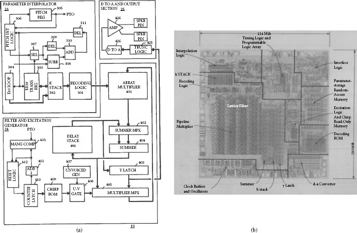
The architecture of the Speak & Spell DSP resulted from the collaboration of two individuals. One was Richard Wiggins, a new TI employee who was a speech research scientist. The second was a calculator integrated circuit architect named Larry Brantingham. Their job was to make the Speak & Spell product talk. The concept was to use linear predictive coding (LPC) with ten coefficients [4,5]. To achieve this, the team was required to use a very complex process known as 7 μM PMOS. Figure 1.1 shows a block diagram of the architecture and a die photo of the TMC0280 device.
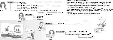
Before jumping into the programmable DSP devices that TI introduced, here is a perspective that may help you while reading this chapter. It is material excerpted from a book about the history of TI’s DSP devices [6]. The main feature of the book was the inclusion of an actual die from each generation of DSP. The book referred to the four dynasties of TI’s product line. The next section discusses the background of the Speak & Spell and the development of the dynasties as detailed in Reference [6].
1.3 INTRODUCTION TO FIXED POINT DSPS
The Speak & Spell DSP was a fixed function device that performed only LPC-10 speech synthesis. It was obvious to several TI designers that although the TMC0280 was very successful, the next device needed to be more flexible. Specifically it needed to go beyond speech synthesis and perform speech analysis for vocoding, speech recognition, and speaker identification. Several design teams began architectural development of the next device. TI’s Educational Products Division wanted a follow-on device to create products using speech encoding to further enhance its learning aid product line. Another team worked on a more general purpose architecture that could be programmed for speech algorithms and perhaps telecommunications algorithms.
FIGURE 1.1 (a) Block diagram of TMC0280 Speak & Spell speech synthesizer from U.S. Patent 4,209,836. (b) Die photo of device.
After great numbers of interactions among device architects, the final decision was to focus on the architecture that showed the greatest flexibility. The choice was to modify a Harvard [21] architecture having 32-bit instruction words and 16-bit data words. The Harvard architecture was chosen because (1) it was the architecture chosen for the TMS1000 microcontroller product line TI already had in production; and (2) it could use the instruction and data buses after minor modifications to act as data buses that allowed simultaneous feeding of both the multiplier and multiplicand to the hardware multiplier. TI cited the “Modified Harvard” architecture in its market communications [22].
1.3.1 TMS32010
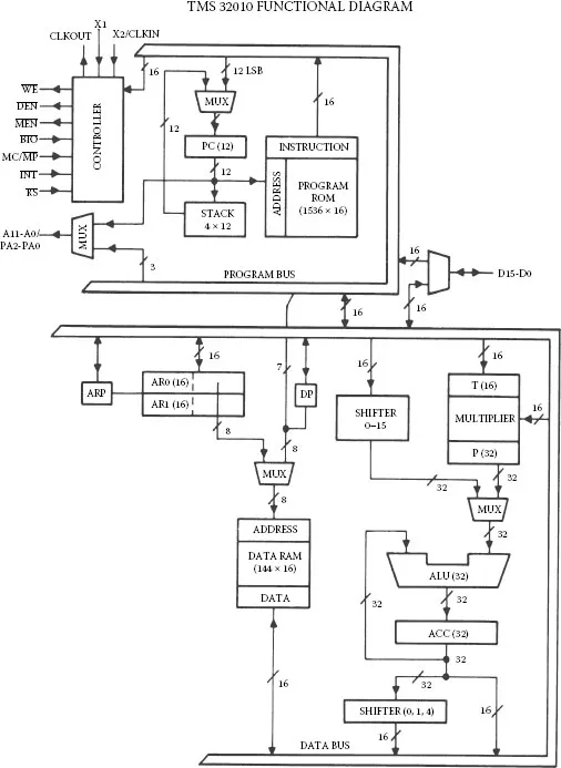
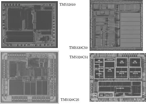
The first programmable DSP known as the TMS32010 (Figure 1.2) was introduced at the International Solid-State Circuits Conference (ISSCC) in 1982 [7]. Figure 1.3 makes it easy to describe the architecture by dividing the die into four quadrants: CPU, RAM, ROM, and multiplier. Later in the chapter we will show die photos of later generation DSPs in which the multipliers are not easily detectable because of size reductions resulting from greater density achieved by advanced integrated circuit fabrication processes.
One heated architectural arguments concerned the need for interrupts. The initial design did not have an interrupt based on the very simple reasoning that realtime systems, by definition, could not be interrupted. The argument was settled by including an interrupt that could be polled by the CPU when it was not involved in a real-time process.
Until then, all TI’s processors had two versions—one for development and one for production. The emulator was designed to allow system designers to design and debug their products. The second (production) device was used in the manufacturing of their end products. The TMS32010 was to be one of the first self-emulation devices. That meant the 2.5 K on-chip ROM could be replaced by external SRAM until the code was mature enough to create a ROM at mask level to program the on-chip memory. When we learned that many of our customers used the emulation mode to turn a ROM-based device into a RAM-based device, we realized we were more brilliant than we thought.
One last point must be made about the size of the on-chip RAM—it was only 144 words. The two reasons for choosing that RAM size were (1) we ran out of die size to increase, and (2) the chosen size was large enough for a 64-point FFT and still allowed sixteen words of scratch pad memory for the programmer to use. The CMOS versions of the TMS32010 were expanded to 256 words of on-board RAM.
Figure 1.2 is a block diagram of the TMS32010 architecture [7]. Table 1.1 lists the various generations and a few design details of the fixed point DSPs marketed by TI. The list in Table 1.1 is by no means complete. TI continues production of many of the devices in these product families. Further, the TMS320C25 was the first in a family of digital signal controllers designated the C24x, C27x, and C28x. They are now known as microcontrollers. The TMS320C50 device allowed TI to enter the digital cell phone market and began a family of phone architectures (C54x, C55x, and OMAP). I’ll discuss the OMAP architecture in Section 6.1 covering multi-processing.
FIGURE 1.2 TMS32010 block diagram.
The birth of the digital cellular phone market finally drove TI to focus on power dissipation as a performance metric. The focus actually started in the DSP product team a few years earlier.
FIGURE 1.3 Die photos of TMS32010, TMS320C25, TMS320C50, and TMS320C51.
Sometime in the late 1980s, a customer called us about our fi...