- 480 pages
- English
- ePUB (mobile friendly)
- Available on iOS & Android
eBook - ePub
Particle Control for Semiconductor Manufacturing
About this book
There is something Alice-in-Wonderlandish about powerful and vital computer systems being shut down by a microscopic mote that a hay-feverist wouldn't sneeze at, but as computer chips get smaller, smaller and smaller particles on their surface have a larger and larger effect on their performance. In
Trusted by 375,005 students
Access to over 1.5 million titles for a fair monthly price.
Study more efficiently using our study tools.
Information
1. PARTICLE INTERACTION WITH INTEGRATED CIRCUITS
INTRODUCTION
This chapter is a qualitative and quantitative overview of the effects of particles on integrated circuits. First is a review of the various ways that particles can cause yield loss on integrated circuits. In particular, there are several ways that particles can cause damage that have only recently been recognized as important by particle control technologists. By some of these mechanisms, the circuit may be damaged by particles so small that they were previously thought to be of little concern.
Particle-integrated circuit interactions will then be reviewed quantitatively. Basic information on yield models will be presented, along with the effect of nonuniform distributions of defects on the yield model.
An excellent introduction to the problems caused by particles in integrated circuit manufacturing has been given by Cooper (1986), and a qualitative description of the various ways that particles can cause defects on integrated circuits is reviewed in a previous article by the author (Fisher, 1987). One example of a defect caused by a particle is where the particle itself is the defect and causes failure of the circuit by disruption of the pattern or by bridging separated features. Particle-caused defects include the shorting of two conductors by a particle and open circuits in the same features.
Another example of a defect caused by a particle is where the particle causes a defect that remains even after the particle is gone. Defects of this type commonly occur when the particle masks an area of the circuit that should not have been masked by photoresist or some other masking layer. An area may also be unmasked that should have been masked if the particle leaves a hole in a photoresist pattern. If an area is masked prior to an etching step, it may not be etched as intended. If the area is unintentionally exposed. material may be etched away where it was supposed to remain. Prior to an implantation step, a masked area may not be doped as intended. An exposed area may be implanted when it should not be.
In the two examples just cited, a particle is itself a defect or a particle causes a defect that remains even after the particle is gone. Both of these cases result from a physical or mechanical interaction of particles with the integrated circuit. In these cases, the size of the particle relative to the circuit feature size is a major factor in determining whether the particle causes a defect or not. A rule of thumb often applied is that the particle must be some fraction of the minimum circuit feature size to be large enough to cause a killing defect. Commonly this fraction is taken to be 1/10. Because the minimum feature sizes on the most advanced products are near 1 μm, particles near 0.1 μm are now of concern. Feature sizes will undoubtedly decrease, so ever smaller particles will be a problem.
DEFECTS CAUSED BY PARTICLES < 0.1 μm
In addition to the two familiar physical or mechanical defect-causing mechanisms described above, particles much smaller than the minimum circuit feature size may cause killing defects in other ways through both physical or mechanical and chemical interactions. These include particle interactions with thin layers, chemical interactions, and particle-induced defects where the resulting defect is much larger than the particle itself.
If a particle causes a defect in a thin layer, it is the particle size relative to the layer thickness that determines if the defect is killing, rather than the particle size relative to a circuit feature size. Much smaller particles can cause killing defects in circuits by disruption of thin layers than by the previously described mechanisms because layer thicknesses may be much less than minimum feature sizes in the plane of the wafer. For example, the gate or capacitor oxide thicknesses in MOS devices may be as thin as 100 Å(0.01 μm) in circuits with minimum feature sizes of 1 μm. A particle with a diameter of only 100 Ais large enough to bridge this oxide. The interaction of small particles with thin layers may be either physical or chemical.
Particle defects occur through chemical interactions when the particle chemically reacts with circuit features. One example is the formation of a conducting region in an insulator when the particle reacts with it, such as with silicon dioxide during growth of a gate oxide. A particle much smaller than the gate oxide thickness may cause a defect in the oxide by inhibiting or enhancing the formation of the oxide during thermal oxidation. Or, silicon may be unintentionally doped by particles containing elements that are electrically active in silicon. An example is the formation of conductive regions between the collector and emitter of bipolar transistors that short the two regions together.
When a particle causes a defect by chemical means, the chemical identity of the particle is more important than the particle size. This is in contrast to physical or mechanical defect-causing mechanisms where the particle size is more important than the chemical identity. The relative importance of the size and composition for the two mechanisms is summarized in the following table.
Particle size | Chemical composition | |
Physical interaction | More important | Less important |
Chemical interaction | Less important | More important |
A final case of defect formation by a very small particle occurs when a defect is formed in such a manner that the defect is much larger than the particle. An example is when a small particle masks the etching of a layer that is much thicker than the diameter of the particle. If the etching is very anisotropic, the layer under the particle will not be etched, leaving a pillar of unetched material much larger than the particle. The interaction to cause this type of defect is physical. Another example is the formation of a large defect in a silicon epitaxial film nucleated by a small particle in the film during its growth.
PROBABILITY OF DEFECT FORMATION
The probability that a given particle causes a killing defect depends on:
• Interaction mechanism—physical or chemical,
• Size of the particle,
• Chemical identity of the particle,
• Where the particle falls on the circuit, the sensitive area, and
• Point in the process where the particle falls on the circuit, and how long it stays there.
For each interaction mechanism, some particles are so large that they will always cause a defect, and some are so small that they will never cause a defect. The general shape of the curve describing the probability of failure as a function of the defect size is shown below. (Also see Stapper, Armstrong, and Saji, 1983.)
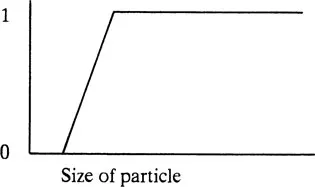
The exact shape of this curve depends on the circuit design and specifics of the manufacturing process. The exact sizes of particles that never or always cause defects depend on the interaction mechanism. For each circuit, process, and interaction mechanism, there is a different curve.
Each circuit has some areas that are insensitive to particles. A particle in these areas is very unlikely to cause a killing defect. These include the bonding pads, alignment marks, and test structures on the circuit. Other insensitive areas on the wafer include unused area at the wafer circumference and scribe line areas.
Finally, there are many points in an integrated circuit manufacturing process where particles may come and go without causing a killing defect. One example is a particle that is part of a photoresist masking layer that is removed with the resist when the resist pattern is no longer needed. Another is a particle that is deposited during one process step, then removed during a cleaning step that immediately follows.
QUANTITATIVE EFFECT OF PARTICLE DEFECTS ON YIELD
Qualitative descriptions of the effect of particle defects on integrated circuit yield allow us to judge the probability that a given particle causes yield loss or not. The quantitative dependence of the yield of integrated circuits on the defect density of the circuit may be described by yield models. The referenced article by Stapper, Armstrong, and Saji (1983) summarizes the derivation of several yield models in detail.
Yield models are studied primarily because of their economic importance. They may be used to predict the yield of new technologies or to forecast the results of process improvements. They illustrate that yield decreases rapidly as defect density rises, and that yield decreases rapidly as chip area increases.
We must first distinguish between point defects that may be caused by particles, and gross or area defects that have other causes. Area defects are those that cause failures of all the chips in areas that are large compared to the area of an individual chip, such as a whole wafer or half a wafer, or of several wafers in a lot of wafers. These failures usually result from gross misprocessing, such as mask misalignment or the use of a wrong mask, a missing or double ion implantation, an incorrect film thickness, over or under etching, or incorrect substrate resistivity or type. The yield loss from broken or lost wafers may also be included in this type of yield loss.
Yield loss due to gross or area defects is not a function of the point defect density, so they are not accounted for by models that assume point defects. In practice, the yield loss due to incorrectly processed wafers or lots of wafers is accounted for by a multiplicative factor to determine the overall yield of a processing line.
One model for the dependence of yield on the point defect density assumes a random distribution of the defects, where the probability of the occurrence of a defect on a chip is independent of the location of any of the other point defects (a Poisson distribution). This distribution of defects leads to the expression for the yield:
(1-1) |
where
Y = yield, or fraction of circuits that do not have a defect,
D = defect density, and
A = area of the circuit.
Note that the product of the defect density and the circuit area, DA, is the number of defects per chip. This model predicts an exponential decrease of yield with defect density and with chip area, so that the yield falls dramatically as either of these two functions increases.
Fortunately, the distribution of defects on circuits is generally not random, and this nonrandom distribution leads to real device yields that are higher than those predicted using Poisson statistics. Variations in the defect density occur within individual wafers, from wafer to wafer within a lot of wafers, and from lot to lot. These variations occur because it is unlikely that any two parts of a wafer, any two wafers in a lot, or any two lots of wafers experience exactly the same conditions during processing. For example, in a cassette of wafers being loaded into a processing machine, an end wafer may be exposed for a longer period of time to clean room air, and the end wafer may shield adjacent wafers from particle deposition from the air.
The yield is higher when the defect distribution is not random than when it is random because ther...
Table of contents
- Cover
- Half Title
- Title Page
- Copyright Page
- Table of Contents
- Preface
- 1 Particle Interaction with Integrated Circuits
- 2 Introduction to Particle Science
- 3 Particle Size Distributions
- 4 Light Scattering Theory
- 5 Developing Trust in Particle Counters
- 6 Ultrafine (<0.1-μm Diameter) Particles
- 7 Particle Control Methods: I
- 8 Predicted and Measured Clean-Room Contamination
- 9 The Dynamics of Aerosols in Clean-Room Environments: Implications for Monitoring and Control of Airborne Particles and Their Sources
- 10 Measurement and Minimization of Particles in Process Gases
- 11 Particles in Process Liquids
- 12 The Immersion Wet Process System
- 13 Measurement of Particles from Equipment and Processes: the Particles-per-Wafer-per-Pass (PWP) Method
- 14 Measurement of Particle Emission Rates from Equipment
- 15 Survey of Process-Induced Defects
- 16 Particle Control Methods: II
- 17 Clean Equipment Design Rules and the SMIF Isolation Concept
- 18 Airflow Modeling and Particle Control by Vertical Laminar Flow
- 19 Particle Deposition Data: Room Air Ionization as a Control Method
- 20 Particle Identification
- 21 Particle Adhesion to Surfaces: Theory of Cleaning
- 22 Experimental Evaluation of Cleaning Techniques
- 23 Wafer Cleaning: Present and Future
- 24 Equipment Cleaning to Minimize Particle Deposition
- 25 Review of FED-STD-209D
- 26 Methods of Circuit Defectivity Analysis
- Index
Frequently asked questions
Yes, you can cancel anytime from the Subscription tab in your account settings on the Perlego website. Your subscription will stay active until the end of your current billing period. Learn how to cancel your subscription
No, books cannot be downloaded as external files, such as PDFs, for use outside of Perlego. However, you can download books within the Perlego app for offline reading on mobile or tablet. Learn how to download books offline
Perlego offers two plans: Essential and Complete
- Essential is ideal for learners and professionals who enjoy exploring a wide range of subjects. Access the Essential Library with 800,000+ trusted titles and best-sellers across business, personal growth, and the humanities. Includes unlimited reading time and Standard Read Aloud voice.
- Complete: Perfect for advanced learners and researchers needing full, unrestricted access. Unlock 1.5M+ books across hundreds of subjects, including academic and specialized titles. The Complete Plan also includes advanced features like Premium Read Aloud and Research Assistant.
We are an online textbook subscription service, where you can get access to an entire online library for less than the price of a single book per month. With over 1.5 million books across 990+ topics, we’ve got you covered! Learn about our mission
Look out for the read-aloud symbol on your next book to see if you can listen to it. The read-aloud tool reads text aloud for you, highlighting the text as it is being read. You can pause it, speed it up and slow it down. Learn more about Read Aloud
Yes! You can use the Perlego app on both iOS and Android devices to read anytime, anywhere — even offline. Perfect for commutes or when you’re on the go.
Please note we cannot support devices running on iOS 13 and Android 7 or earlier. Learn more about using the app
Please note we cannot support devices running on iOS 13 and Android 7 or earlier. Learn more about using the app
Yes, you can access Particle Control for Semiconductor Manufacturing by R.P. Donovan in PDF and/or ePUB format, as well as other popular books in Technology & Engineering & Chemistry. We have over 1.5 million books available in our catalogue for you to explore.