- 559 pages
- English
- ePUB (mobile friendly)
- Available on iOS & Android
eBook - ePub
Photovoltaic Engineering Handbook
About this book
The Photovoltaic Engineering Handbook is the first book to look closely at the practical problems involved in evaluating and setting up a photovoltaic (PV) power system. The author's comprehensive knowledge of the subject provides a wealth of theoretical and practical insight into the different procedures and decisions that designers need to make. Unique in its coverage, the book presents technical information in a concise and simple way to enable engineers from a wide range of backgrounds to initiate, assess, analyze, and design a PV system. It is beneficial for energy planners making decisions on the most appropriate system for specific needs, PV applications engineers, and anyone confronting the practical difficulties of setting up a PV power system.
Trusted by 375,005 students
Access to over 1.5 million titles for a fair monthly price.
Study more efficiently using our study tools.
Information
Subtopic
Optics & LightPart I
Technological Processes
1 Solar Cell Technologies
1.1 INTRODUCTION
It has been over 150 years since Becquerel in 1839 first discovered that a photovoltage was developed when light was directed onto one of the electrodes in an electrolyte solution. Adams and Day were the first to observe the photovoltaic (PV) effect in a solid (selenium) in 1877. Early solid-state researchers including Lange, Grondahl and Schottky did pioneering work on selenium and cuprous oxide PV cells. However, it was not until 1954 that scientific literature published results on the use of the PV effect in energy conversion processes.
The wide spectrum of semiconductor-related technologies encompasses the field of solar cells (see figure 1.5) and all manufacturing processes described below are derived from and enjoy the latest advances made in microelectronics. From this point of view, PV converters belong to the so-called high-technology field and any improvement in that field contributes to the progress in semiconductor technology as a whole.
The silicon solar-cell-manufacturing process involves basically three stages.
(i) | Material preparation and shaping. |
(ii) | Cell processing. |
(iii) | Cell interconnection and encapsulation. |
The conventional technological process, the flow chart of which is presented in figure 1.1, relies conventionally on the high-purity semiconductor-grade silicon (SG-Si) available from electronics industry wastes. In this process, quartzite as a raw material is reduced into metallurgical-grade silicon (MG-Si), the purity of which lies in the 98–99% range. MG-Si is purified to qualify as the so-called SG-Si or electronic-grade silicon (EG-Si). SG-Si is then melted in a crucible and pulled out to form a single-crystal silicon ingot by using the traditional Czochralski (CZ) technique (figure 1.2). Ingots are cut into wafers which are etched to remove the damage induced during the slicing operation. Wafers are then processed into a complete solar cell (figure 1.3), i.e. junction diffusion, contact elaboration and anti-reflection coating. Finally, cells are interconnected to achieve a practically useful voltage and encapsulated into a module by using a lamination technique.
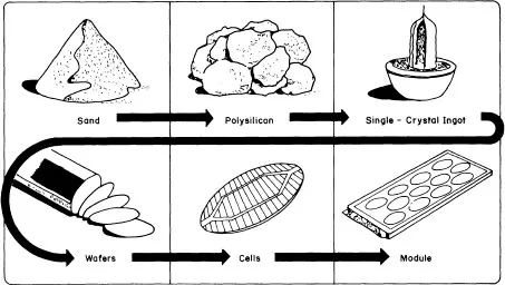
Figure 1.1 Solar-cell-manufacturing process.
In 1982, silicon material contributed nearly 50% of the total cost of a PV module whereas cell processing and module assembly contributed respectively 30% and 20% of the total cost breakdown. Since that time, critical paths in the silicon technology process have been investigated intensively, leading to major technical breakthrough and substantial cost reduction as well as the definition of various specific silicon routes for solar cell fabrication (figures 1.4 and 1.5).
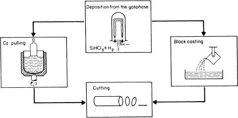
Figure 1.2 Production and slicing of silicon ingots.
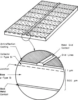
Figure 1.3 A typical single-crystal silicon p–n junction solar cell.
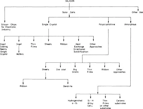
Figure 1.4 Silicon and its various routes of utilization, particularly the solar-cell route.
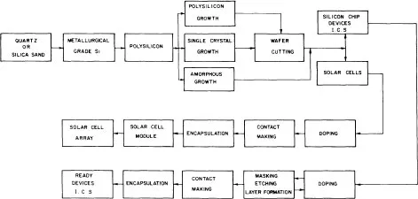
Figure 1.5 Spectrum of silicon technology.
A review of recent progress includes the following.
(i) Material.
(a) Preparation and definition of ‘solar-grade’ silicon (SOG-Si) material as a low-cost and solar-specific alternative to the expensive semiconductor-grade material which will soon be depleted.
(b) Development of the polycrystalline technology route based on SOG-Si as an industrial alternative to the single-crystal technology and including the ingot-casting technique, optimized slicing techniques and, in particular, the continuous process to replace batch processes.
(c) Research and development efforts in sheet technology (ribbon, foil, thick films, etc).
(ii) Cell processing.
(a) Surface texturization to decrease optical losses in single-crystal cells.
(b) Cold-junction processing (CJP) in which doping impurities are introduced by ion or molecular implantation or evaporated or spray deposited on the wafer surface. They are then driven into the material to form a p–n junction by pulsed annealing (laser or electron beam); this process is amenable to full automation.
(c) Screen printing and to a lesser extent electroplating for deposition of contacts. Research is being carried out to replace noble materials (silver) by low-cost alternative materials (aluminium).
Moreover, substantial cost reductions have been achieved through process automation, and it is widely recognized that the industrial dimension is of paramount importance for the economic use of PV converters.
A further cost reduction scenario implies more fundamental changes and, in the year 2000, amorphous silicon (a-Si) (or other material) thin-film technology is anticipated to emerge as a key technology for future low-cost mass production of solar cells. In the last few years, remarkable progress has been seen in both physics and technology development of hydrogenated amorphous silicon (a-Si:H) solar cells which in a very short period has moved through all the phases from discovery to industrial production. Nowadays a-Si solar cells have a considerable market size particularly in the consumer electronics field such as pocket-sized calculators, wrist watches and battery rechargers. Although a-Si technical readiness has still to be proven to enter the power production sector, the basics of the process are reviewed in the present chapter.
1.2 LARGE-SCALE PRODUCTION OF SILICON BASE MATERIAL
1.2.1 Conventional technology process
1.2.1.1 Quartzite to metallurgical-grade silicon
After oxygen, silicon is the most abundant element in the Earth’s crust. Geological processes have provided different ways of concentrating silicon dioxide in vast deposits all over the world. Quartzite rock and special strata of quartz sand have been the most widely used raw materials for the production of elemental silicon. Their inexpensive mining requires little energy and has negligible environmental impact. The quality ranges of either genuine or refined silicon dioxide have been computed in table 1.1. The preference or necessity to use a certain quality depends largely on the type of reduction and refining process sequence and possibly the geographical situation. Prices of quartz product can be 50 times more expensive when obtained from rock crystal (US$0.2 kg−1 in 1979) as opposed to selected quartz sand.
Table 1.1 Different types of SiO2 sources.
Mining product | Upgrading | Nature of particles | Impurities (wt.%) |
Quartzite rock | Standard (technical grade) | Chunks | ≈ 1 |
Special silicates | Chemical conversion | Powder | <0.3 |
Quartz sand | Standard (technical grade) | Grains | <0.2 |
Selected quartz sands, pegmatites | Chemomechanical treatment | Grains | <0.05 |
Special quartz veins, rock crystal | Standard | Nuggets | <0.03 |
Present commercial extraction processes use the crystalline form of silicon dioxide, quartzite, with 90% or more silica (SiO2) rather than sand whose major constituent is also silica. Sand with its high amount of impurities is too costly to process and therefore does not make an economic choice as a raw material. The quartzite is reduced in large arc furnaces (figure 1.6) by carbon to produce elemental silicon according to the following chemical reaction...
Table of contents
- Cover
- Half Title
- Title Page
- Copyright Page
- Dedication
- Table of Contents
- Preface
- Part I Technological Processes
- Part II The Photovoltaic Generator
- Part III Photovoltaic Systems Engineering
- Part IV Characterization and Testing Methods
- Part V Sizing Procedure
- Part VI Economic Analysis
- Part VII Instrumentation
- Index
Frequently asked questions
Yes, you can cancel anytime from the Subscription tab in your account settings on the Perlego website. Your subscription will stay active until the end of your current billing period. Learn how to cancel your subscription
No, books cannot be downloaded as external files, such as PDFs, for use outside of Perlego. However, you can download books within the Perlego app for offline reading on mobile or tablet. Learn how to download books offline
We are an online textbook subscription service, where you can get access to an entire online library for less than the price of a single book per month. With over 1.5 million books across 990+ topics, we’ve got you covered! Learn about our mission
Look out for the read-aloud symbol on your next book to see if you can listen to it. The read-aloud tool reads text aloud for you, highlighting the text as it is being read. You can pause it, speed it up and slow it down. Learn more about Read Aloud
Yes! You can use the Perlego app on both iOS and Android devices to read anytime, anywhere — even offline. Perfect for commutes or when you’re on the go.
Please note we cannot support devices running on iOS 13 and Android 7 or earlier. Learn more about using the app
Please note we cannot support devices running on iOS 13 and Android 7 or earlier. Learn more about using the app
Yes, you can access Photovoltaic Engineering Handbook by F Lasnier in PDF and/or ePUB format, as well as other popular books in Technology & Engineering & Optics & Light. We have over 1.5 million books available in our catalogue for you to explore.