Contents
4.1 Overview
4.2 Introduction: Challenges of Conventional CMOS Technology
4.3 Gate-Length Scaling in Fully Depleted Devices
4.4 Planar Fully Depleted Devices
4.4.1 Process Challenges
4.4.2 Performance Boosters
4.4.3 Scalability
4.5 FinFETs: Bulk and SOI
4.5.1 Process Considerations
4.5.2 Performance Boosters for FinFETs
4.5.3 Extendibility
4.6 Nanowires and Vertical Transistors
4.7 Conclusions
References
4.1 Overview
In this chapter, we first review the major issues facing conventional complementary metal–oxide–semiconductor (CMOS) scaling. We then introduce the basics of a fully depleted device operation and discuss how fully depleted devices overcome the barriers that limit conventional scaling. In addition, bulk and silicon (Si) on insulator (SOI) FinFETs are compared and contrasted. The attributes of a planar fully depleted silicon on insulator (FDSOI) are reviewed and also compared with FinFETs. Finally, the ultimate fully depleted device option, a nanowire transistor, is presented and its benefits and drawbacks are shown.
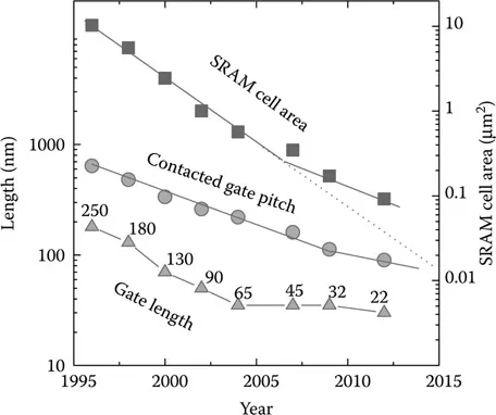
In order to meet the requirement of doubling the transistor density from one node to the next, the contacted gate pitch (CGP) is reduced by 30% per node as shown in Figure 4.1. The lithography community has developed several innovative solutions to pattern features smaller than the wavelength of light using diffraction techniques, immersion lithography, double patterning, cut masks, and other approaches. The advent of extreme ultraviolet (EUV) lithography has also facilitated the miniaturization of critical features. However, the demand on the gate length is particularly challenging. In previous technology nodes, the distances between gates have been large relative to the gate length. In present and future technology nodes, however, the distance between gates is small relative to the gate length itself. This necessitates the need for gate-length scaling. Beyond the physical challenge of shrinking device dimensions, there is a significant challenge to maintain the electrostatic integrity of the transistors. In the past, this was accomplished through gate dielectric scaling, channel doping, and extension optimization. These conventional techniques are no longer capable of controlling short-channel effects. New device architectures are needed to continue the scaling trend. In addition to controlling electrostatics, transistor performance is key to every technology node. Thus, transistors must be simultaneously scaled with good electrostatics as well as performance. This chapter describes the issues associated with conventional scaling and explores the alternatives to conventional scaling.
Figure 4.1 CMOS scaling trend over a period of roughly two decades. The CGP is scaled by 0.7 per node, which enables the total number of transistors to increase by a factor of 2 for a given area. (Note that device isolation and metal pitch are also scaled at roughly the same rate as CGP to enable overall density scaling.) Interestingly, during the period from the 65 nm node to the 32 nm node, the CGP scaled but the gate length did not scale much.
4.2 Introduction: Challenges of Conventional CMOS Technology
For the past several decades, the consumer electronics market has benefited enormously from the continued scaling of semiconductor devices. Additionally, big businesses have enjoyed unprecedented increases in productivity largely due to CMOS scaling. The increased density and miniaturization of transistors due to CMOS scaling have been accomplished through advances in patterning, device design, and process technology. Although CMOS scaling has been an evolutionary process, several abrupt changes have enabled the industry to keep on track.
Table 4.1 Dennard’s Scaling Theory
| Parameter | Scaling Factor |
| Device dimension tox, L, W | 1/k |
| Doping concentration Na | K |
| Voltage V | 1/k |
| Current I | 1/k |
| Capacitance eA/t | 1/k |
| Delay time per circuit VC/I | 1/k |
| Power dissipation per circuit | VI 1/k 2 |
A prescription for conventional scaling was proposed by Dennard et al. in 1974 [1]. The semiconductor industry moved forward for many generations according to Dennard’s scaling theory as shown in Table 4.1. The major benefits of scaling are that the circuits switch faster with less power consumption and device dimensions scale so circuit density increases. The industry followed this scaling theory for several decades.
One of the hallmarks of scaling is that the distance between transistors or CGP decreases for every generation of technology and this enables a significantly smaller static random-access memory (SRAM) cell size. A plot of the gate length, CGP, and the SRAM cell size as a function of technology node and year is shown in Figure 4.1. As the gate length decreases, however, it becomes more challenging to maintain electrostatic control of the gate over the channel and the transistor becomes more difficult to turn off. In order to prevent this, electrostatics or short-channel effects can be controlled by thinning the gate dielectric to provide stronger coupling between the gate and the channel. The channel doping (halo dose) can also be increased to control the short-channel effects and the source–drain (S/D) extension junctions can be made shallower to reduce the influence of the drain potential on the channel.
Figure 4.1 shows significant gate-length scaling from the 250 to the 65 nm node. However, a dramatic slowdown of gate-length scaling from the 65 to the 22 nm node can also be observed. This slowdown is in part due to the physical limitation of gate dielectric scaling. When a conventional SiO2 gate dielectric is scaled below about 2.0 nm, it must be heavily nitrided or it will not pass reliability requirements. Also, gate leakage can be excessive at these thin film thicknesses. Nitrided gate dielectrics are used to scale the equivalent oxide thickness (EOT) to about 1.2 nm with acceptable reliability and gate leakage. The slowdown in gate dielectric scaling not only prevents appreciable gate-length scaling but also poses a significant challenge for device performance. Drive current and gate dielectric scaling are nearly linearly proportional. That is, when the gate dielectric gets thinner, the drive current increases. Although advancements in high-κ gate dielectrics have enabled some gate-oxide scaling, this scaling may not be a consistently sustainable element leading to continued gate-length scaling. The CGP requirement for nodes beyond 22 nm requires gate-length scaling to ensure that the gate can fit into the pitch. This problem has been temporarily put on hold with the advent of self-aligned contacts. However, gate-length scaling is needed for advanced technology nodes.
Conventional device design methodology seeks to scale gate length while enabling higher drive currents with fixed or lower off-currents. If S/D extensions can be made shallower through advanced doping and annealing then the gate can gain more control over the channel and the gate length can be scaled. In addition, if the S/D extensions can be made more abrupt, they can be placed in closer proximity to the channel and the drive current can be increased due to the enhanced coupling between the inversion layer and the extension when the transistor is turned on. The halo, which is opposite-type doping compared with the extension, can also help to form an abrupt extension by cutting the tail of the extension. That is, the extension tail can diffuse and extend into the channel. The halo can counteract the electrical effects of the diffuse extension tail, thereby forming a more abrupt extension. However, channel or halo doping has several detrimental effects. First, as the gate gets smaller, more halo doping is needed to help control the charge sharing between the source and the drain. This higher channel doping leads to mobility degradation. If the channe...