![]()
1
Thin-Film Sensors Integrated in Information Displays
Mutsumi Kimura
CONTENTS
1.1 Introduction
1.2 p/i/n Thin-Film Phototransistor
1.2.1 Fabrication Processes and Device Structures
1.2.2 Comparison of Thin-Film Photodevices
1.2.3 Device Characterization of the p/i/n Thin-Film Phototransistor
1.3 1-Transistor 1-Capacitor Type Temperature Sensor
1.3.1 Fabrication Processes and Device Structures
1.3.2 Temperature Dependences of Transistor Characteristics
1.3.3 Cell Circuit and Driving Method
1.3.4 Experimental Results
1.4 Ring Oscillator Type Temperature Sensor
1.4.1 Fabrication Processes and Device Structures
1.4.2 Temperature Dependences of Transistor Characteristics
1.4.3 Ring Oscillator Circuit
1.4.4 Experimental Results
1.5 Magnetic Field Sensor
1.5.1 Matrix Array of Poly-Si Micro-Hall Devices
1.5.2 Compensation Technique of Characteristic Variation
1.5.3 Area Sensing of Magnetic Field
1.6 Conclusion
References
Thin-film transistors (TFTs) have been widely utilized for flat-panel displays (FPDs). The essential feature is that functional devices can be fabricated on large flexible substrates at low temperature at low cost. The outstanding advantage can be employed in sensor applications and maximized when they are integrated in FPDs. Here, first, we propose a p/i/n thin-film phototransistor as an excellent thin-film photodevice. Next, we compare two types of temperature sensor, 1-transistor 1-capacitor (1T1C) type and ring oscillator type, whose sensitivities are roughly 1°C. Finally, we also propose a magnetic field sensor using a micro-Hall device, which realizes real-time area sensing of a magnetic field.
1.1 INTRODUCTION
Thin-film transistors (TFTs) [1, 2] have been widely utilized for flat-panel displays (FPDs) [3], such as liquid crystal displays (LCDs) [4], organic light-emitting diode (OLED) displays [5], and electronic papers (EPs) [6]. They have been recently applied to driver circuits, system-on-panel units [7], and general electronics [8], such as information processors [9], integrated in the FPDs. However, the essential feature of the thin-film technology is that functional devices, such as active-matrix circuits, amplifying circuits, and general circuits, can be fabricated on large and flexible substrates at low temperature at low cost. This outstanding advantage can be employed in not only the FPDs, but also sensor applications because the active-matrix circuits are required for some kinds of area sensors, amplifying circuits are necessary to amplify weak signals from sensor devices, large areas are sometimes needed to improve the sensitivities, and flexible substrates are convenient when they are put anywhere on demand. Moreover, this advantage can be maximized when they are integrated in the FPDs because the thin-film sensors and TFTs can be simultaneously manufactured using the compatible fabrication process. Therefore, we have studied potential possibilities of the thin-film sensors based on TFT technologies [10].
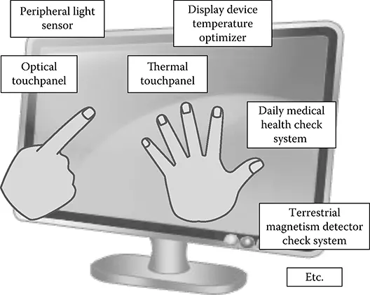
In this article, as examples of the thin-film sensors, we introduce a photosensor, temperature sensor, and magnetic field sensor. First, we propose a p/i/n thin-film phototransistor (TFPT) [11], compare it with other photodevices [12], characterize it from the viewpoint of the device behavior [13], and conclude that the p/i/n TFPT is an excellent thin-film photodevice. Examples for the application of the thin-film photodevices integrated in FPDs are a peripheral light sensor to control brightness of FPDs and an optical touchpanel. The p/i/n TFPTs are also promising for artificial retinas [14, 15, 16, 17, 18, 19, 20 and 21], which is not explained here. Next, we contrive two types of temperature sensor, 1-transistor 1-capacitor (1T1C) type [22] and ring oscillator type [23], and compare them. It is known that the TFTs have temperature dependence of the current-voltage characteristic. We employ the temperature dependence to realize the temperature sensor, and invent a sensing circuit and sensing scheme. It is confirmed that the temperature sensitivities of these temperature sensors are less than 1°C. The 1T1C type temperature sensor has a simple circuit configuration, but it is needed to equip analog voltage sensing circuits, which are fairly complicated circuits and difficult to be integrated on the FPDs using TFTs. On the other hand, the ring oscillator type temperature sensor is available as a digital device. Generally, digital devices are superior to analog devices from the viewpoint of the onward signal operation. Examples for the application of the temperature sensors integrated in FPDs are a temperature sensor to optimize driving conditions and compensate temperature dependences of display characteristics of liquid crystals or organic light-emitting diodes, a thermal touchpanel, and a daily medical health check system. Finally, we also propose a magnetic field sensor using a micro-Hall device based on the Hall effect in the magnetic field [24], which realizes real-time area sensing of the magnetic field [25]. Although there remains room for improvement of the sensitivity, no other devices can realize real-time area sensing of the magnetic field. An example for the application of the magnetic field sensors integrated in FPDs is a terrestrial magnetism detector to know the bearing. Figure 1.1 shows the application of the thin-film sensors integrated in the FPDs.
FIGURE 1.1 Application of the thin-film sensors integrated in the FPDs.
1.2 P/I/N THIN-FILM PHOTOTRANSISTOR
1.2.1 FABRICATION PROCESSES AND DEVICE STRUCTURES
Figure 1.2 shows the device structure of the p/i/n TFPT. The p/i/n TFPT is fabricated on a glass substrate using the same fabrication processes as low-temperature poly-Si (LTPS) TFTs [26, 27 and 28]. First, an amorphous-Si film is deposited using low-pressure chemical vapor deposition (LPCVD) of Si2H6 and subsequently crystallized using a XeCl excimer laser to form a 50 nm thick poly-Si film. Next, a SiO2 film is deposited using plasma-enhanced chemical vapor deposition (PECVD) of tetraethylorthosilicate (TEOS) to form a 75 nm thick control insulator film. A metal film is deposited and patterned to form a control electrode. Afterward, phosphorous ions are implanted through a photoresist mask at 55 keV with a dose of 2 × 1015 cm–2 to form an n-typ...