
eBook - ePub
Embedded Systems Design with 8051 Microcontrollers
Hardware and Software
- 432 pages
- English
- ePUB (mobile friendly)
- Available on iOS & Android
eBook - ePub
About this book
A presentation of developments in microcontroller technology, providing lucid instructions on its many and varied applications. It focuses on the popular eight-bit microcontroller, the 8051, and the 83C552. The text outlines a systematic methodology for small-scale, control-dominated embedded systems, and is accompanied by a disk of all the example problems included in the book.
Trusted by 375,005 students
Access to over 1.5 million titles for a fair monthly price.
Study more efficiently using our study tools.
Information
Chapter 1
BASIC CONCEPTS
The full understanding of microcontrollers and their applications demands knowledge of all aspects of digital systems, from logic gates to microcomputers. In this chapter we outline the basic features of logic gates and memory elements. We use these components to design combinational and sequential logic circuits. Next, we briefly discuss memories and microprocessors to be able to deal with microcomputers. In section 1.8 we explain the basic characteristics of the microcontrollers. Also, we introduce a flag’s taxonomy and symbols which are in use throughout the book. Finally, we discuss embedded applications and the impact of the Internet expansion on future designs.
1.1 Logic gates
Logic gates are the essential building blocks of the digital systems. Figure 1.1 shows basic logic functions and the logic gate symbols. Furthermore, the correspondence input – output values are presented in truth tables. Finally, Figure 1.1 depicts the logic equations consistent with Boolean algebra laws.
For example, the first logic gate is an inverter. The inverter has an input A and an output Y. The next gate computes a little more complex function called AND. The output of the AND gate will be 1 when both inputs are 1. Watch out for a small detail: the AND symbol A could be omitted in the formula.
Naturally, our aim is to be prepared for implementation of any logic function. Having in mind that technology will dictate the most suitable function or functions we need to sort through the possibilities and find functionally complete sets. For instance, the set NOT, AND and OR can be used to form every possible Boolean function. The same applies for NAND or NOR functions.
Figure 1.2 shows a transfer characteristic for the inverter. The transfer characteristic presents the gate output voltage as a function of the input voltage. We can obtain the characteristic by connecting an adjustable voltage source to the gate input and using a voltmeter to measure pairs of input and output voltages.
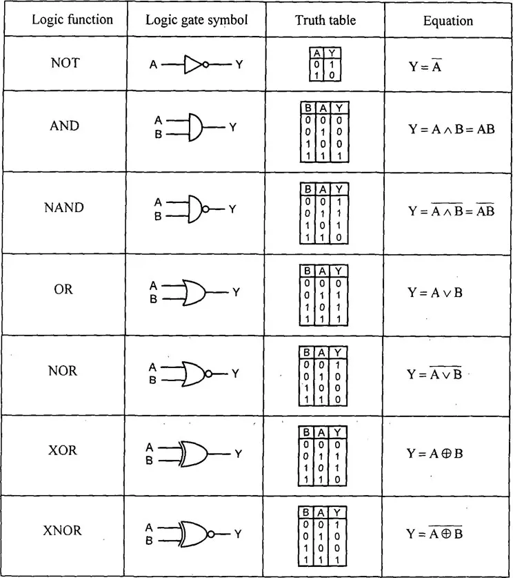
Figure 1.1 Logic functions and logic gates.
The curve displays all possible output voltages. The grid is 1 volt. The logic 1 (high) voltage set is separated from the logic 0 (low) set by a grey area. In a static state gates are not allowed to produce undefined (grey) output voltages. Inevitably, switching from one output level to another will cause the output voltage to pass the grey area.
Furthermore, Figure 1.2 indicates logic levels by the horizontal border lines of the grey area. There are two other logic levels which are relevant for the inputs and can be seen in Figure 1.2 as dashed lines. The differences between the corresponding logic levels are termed noise margins.
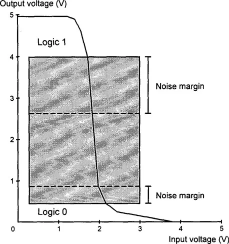
Figure 1.2 Logic levels and the transfer characteristic.
A major parameter which defines the ability of a logic gate to switch fast from one level to another is the delay. The delay is also related to a property called power consumption. Usually, any attempt to decrease the delay leads to increase of the power consumption and vice-versa.
If the logic gates are viewed at a deeper level they can be broken down into two types. First, logic gates built from bipolar transistors are fast, but require relatively more power. Second, logic gates based on MOS (Metal-Oxide Semiconductor) transistors consume less power, however the delays are longer.
The power consumption is crucial in two ways. Obviously, we need to minimize the power used, especially for portable systems. Nevertheless, the power consumption affects the performance indirectly. The logic gates reside in Integrated Circuits (IC). It is imperative for the designers to be able to put as many transistors on a single chip as the application demands. Unfortunately, the ceiling of the heat dissipation limits the number of transistors and therefore the performance.
The density of the integrated circuits can be measured by the number of active elements (transistors) or gates. Figure 1.3 classifies the ICs according to the transistor count. It is certainly implied that the ranges are a general picture rather than strict frames.
Under the MOS technology branch, we distinguish between NMOS and CMOS integrated circuits. The NMOS ICs use n-channel transistors. The CMOS (Complementary MOS) gates are based on pairs of p-channel and n-channel transistors. The key advantage of the CMOS technology is that the circuit consumes practically no power in a static state. The CMOS technology dominates the microcontroller’s market.
Beneath the CMOS branch of the taxonomy tree, we distinguish between static and dynamic logic gate circuits. The dynamic logic circuits depend on the charge of internal capacitors which must be refreshed. A certain amount of the microcontrollers are still produced as dynamic logic devices. As a result, the IC will not operate properly if the clock frequency is below the lower limit.
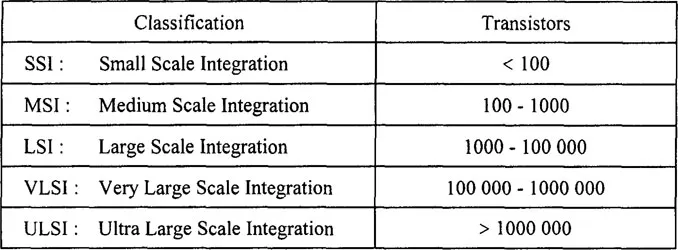
Figure 1.3 An integrated circuits classification.
In contrast, the static CMOS logic, typical for the new microcontrollers, is capable of saving power by decreasing the clock frequency when necessary.
1.2 Combinational logic circuits
Digital systems are built from numerous logic gates. It would be useful for us if we can isolate parts of the system which contain only Combinational Logic Circuits (CLC). The main property of combinational logic is that it has no closed loops or feedback. Breaking down the system into smaller pieces will help us to organize the design process and employ appropriate methods.
Figure 1.4 shows a truth table of an example combinational logic circuit. The circuit is called a decoder. In addition, Figure 1.4 includes the logic equations of this 2-input, 4-output circuit. There are four possible input combinations and each of them activates a single output.
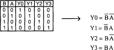
Figure 1.4 The decoder truth table and output equations.
Once we have prepared the logic equations, it is a simple task to draw the decoder combinational logic circuit (network) which can be seen in Figure 1.5. This example circuit consists of two levels of logic gates. The number of levels and the gate delay define the overall delay of the circuit.
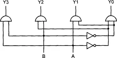
Figure 1.5 The decoder combinational logic network.
A typical application of the decoder is to select memory components according to the current requirements of the system. When a digital system accesses a location in the memory it generates a certain number of signals termed address. The address specifies which memory component is activated and which location in the component is the target. Using the decoder from Figure 1.5 we apply two address signals to the inputs A and B. The outputs YO through Y3 go to the select inputs of the memory integrated circuits.
It is certainly implied that actual designs will deal with mass-produced combinational logic blocks. Figure 1.6 presents a popular 3-line to 8-line decoder 74HCT138. Most obviously, the number of inputs is increased to 3 which brings the number of outputs to 8. In contrast to the previous decoder, the outputs are active low (glance the bubbles) which fits better to the commonly used active low select inputs. Finally, the decoder itself has three select inputs . If the decoder is not selected all outputs are inactive (high) regardless of the inputs A, B and C. In order to select the 74HCT138, both inputs must be tied to the ground and the input tied to high.
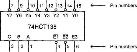
Figure 1.6 The 74HCT138 3-line to 8-line decoder.
You might be surprised when you see the logic symbol of this decoder in different catalogs. In some of them, the output’s letters appear as we show them in Figure 1.6. In some others, the output values are negated in the decoder logic symbol ( through ). What does it mean when the bubbles are still there? The fact is that an asserted output will be at low level. A similar inconsistency in the graphical presentation applies for the select inputs El and E2. Again, the decoder is selected by pins #4 and #5 pulled down and pin #6 pulled up.
The 74HCT138 decoder is a representative of a high-speed CMOS family labelled HCT. The logic levels of this family are the same as the logic levels of the famous Transistor Transistor Logic (TTL).
1.3 Latches and flip-flops
Immediately adjacent to the logic gates are the latches and the flip-flops. The combinational logic circuits could result in useful building blocks, however they do not introduce new fundamental features. But, the latches and flip-flops do. They can be used to store logic values. This distinctive characteristic is achieved by feedback or special design techniques [Wolf 1994a].
There are many types of memory elements as far as the functionality is concerned. Figure 1.7 shows three of the most commonly used memory elements, presented by their state transition tables (functional tables).
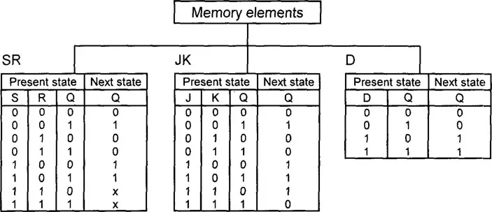
Figure 1.7 Memory elements and functional taxonomy.
• SR memory elements are set by a S input and reset by a R input. When both inputs are not asserted (low) the output Q is not changed. The last two transitions in the table lead to unstable states. Consequently, two active (high) inputs are not allowed.
• JK memory elements are similar to the SR counterparts. As you can see in the table, an input J plays the role of the S input and a K input substitutes for the R input. An advantage of the JK element is that it will be toggled (the state will be changed) if both inputs are asserted high.
• D memory elements have one input. They are also known as delay elements. The output Q copies the input value after some delay.
• Furthermore, in Figure 1.8 we look at the memory elements from a different angle. In this taxonomy we focus on the timing parameters. At the highest level, we distinguish between asynchronous and synchronous memory elements.
• The asynchronous memory elements possess only data inputs. When the pattern of the data inputs is changed, the stored value is also changed and appears at the output after some delay. The asynchronous memory elements are termed latches. An example of an IC which contains four latches is 74LS279 [Texa 1989].
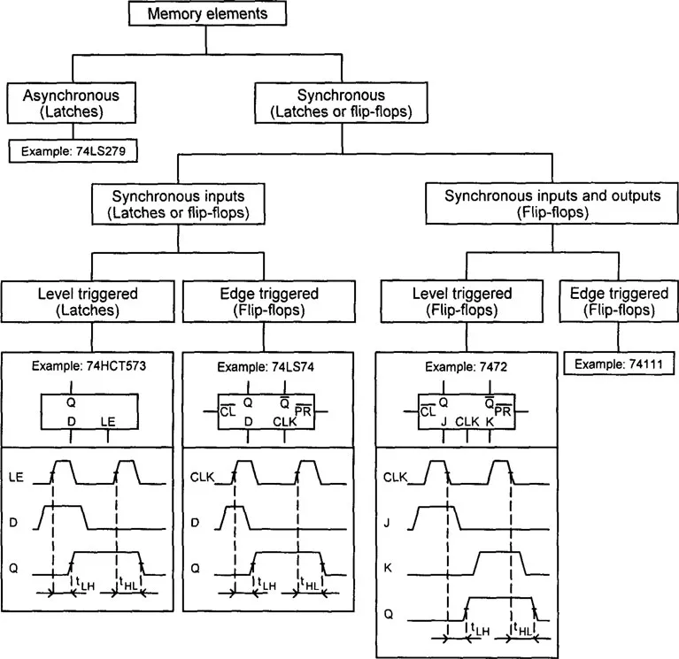
Figure 1.8 Memory elements and timing taxonomy.
• The synchronous memory elements have an extra input called clock input. By means of the clock input two important things can be controlled. First, the access to the memory element is allowed by the clock input. Second, under the synchronous inputs and outputs branch of the taxonomy both inputs and outputs are dependable on the clock input. In other words, we can choose the time when to activate the input circuitry and store the value and when to present the updated value to the output.
The synchronous inputs branch is further classified into level triggered latch...
Table of contents
- Cover
- Half Title
- Title Page
- Copyright Page
- Table of Contents
- Preface
- Chapter 1 Basic concepts
- Chapter 2 The 8051 microcontroller
- Chapter 3 The 8051 assembly language programming
- Chapter 4 Digital interfacing
- Chapter 5 Analog interfacing
- Chapter 6 Interfacing personal computers
- Chapter 7 The 83C552 microcontroller
- Chapter 8 Serial interfaces for distributed embedded systems
- Chapter 9 High level languages for microcontrollers
- Chapter 10 Embedded systems design
- Chapter 11 Design examples
- Appendix A Survey of microcontrollers
- Appendix B The 8051 microcontroller Special Function Registers
- Appendix C The 83C552 microcontroller Special Function Registers
- Appendix D The 8051 and 83C552 microcontrollers instruction set
- Appendix E Instruction set - summary
- Index
Frequently asked questions
Yes, you can cancel anytime from the Subscription tab in your account settings on the Perlego website. Your subscription will stay active until the end of your current billing period. Learn how to cancel your subscription
No, books cannot be downloaded as external files, such as PDFs, for use outside of Perlego. However, you can download books within the Perlego app for offline reading on mobile or tablet. Learn how to download books offline
Perlego offers two plans: Essential and Complete
- Essential is ideal for learners and professionals who enjoy exploring a wide range of subjects. Access the Essential Library with 800,000+ trusted titles and best-sellers across business, personal growth, and the humanities. Includes unlimited reading time and Standard Read Aloud voice.
- Complete: Perfect for advanced learners and researchers needing full, unrestricted access. Unlock 1.5M+ books across hundreds of subjects, including academic and specialized titles. The Complete Plan also includes advanced features like Premium Read Aloud and Research Assistant.
We are an online textbook subscription service, where you can get access to an entire online library for less than the price of a single book per month. With over 1.5 million books across 990+ topics, we’ve got you covered! Learn about our mission
Look out for the read-aloud symbol on your next book to see if you can listen to it. The read-aloud tool reads text aloud for you, highlighting the text as it is being read. You can pause it, speed it up and slow it down. Learn more about Read Aloud
Yes! You can use the Perlego app on both iOS and Android devices to read anytime, anywhere — even offline. Perfect for commutes or when you’re on the go.
Please note we cannot support devices running on iOS 13 and Android 7 or earlier. Learn more about using the app
Please note we cannot support devices running on iOS 13 and Android 7 or earlier. Learn more about using the app
Yes, you can access Embedded Systems Design with 8051 Microcontrollers by Zdravko Karakehayov in PDF and/or ePUB format, as well as other popular books in Technology & Engineering & Electrical Engineering & Telecommunications. We have over 1.5 million books available in our catalogue for you to explore.