![]()
|
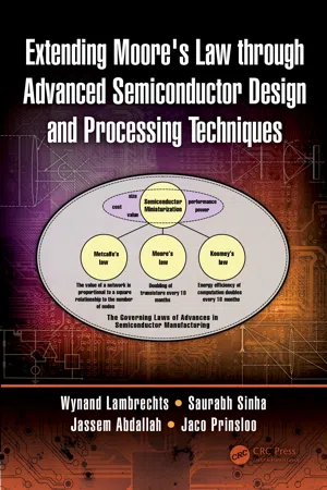
1 | The Driving Forces Behind Moore’s Law and Its Impact on Technology |
Wynand Lambrechts, Saurabh Sinha and Jassem Abdallah
Introduction
The rate of technological advancement as a function of time is governed by the correlation by which the number of components in very large-scale integration (VLSI) integrated circuits (ICs) and their total computing power double approximately every 18–24 months (Moore 1965; Hutcheson 2009). This phenomenon is known as Moore’s law, and was predicted in a 1965 paper by Gordon Moore (Moore 1965), the co-founder of Fairchild Semiconductor and Intel. Moore predicted that the quantity of components integrated into ICs would increase twofold each year for the next decade (from 1965), and ten years later (during 1975), adjusted the prediction to the integrated components doubling every two years. This held true up until the current decade (five decades later), with deviations only occurring recently in response to several factors, primarily physical limitations (at atomic level) and changes in computing habits (such as multicore and open-hardware systems). In 2009, IBM Fellow Carl Anderson noted a trend of semiconductor technology maturing and exponential growth slowing down, similar to that of the railroad, the automotive industry and aviation before it. Moore’s law is related to the scaling law founded on the work of Dennard (1974), known as Dennard scaling. Dennard scaling is specifically related to power scaling in complementary metal-oxide semiconductor (CMOS) transistors. Essentially, the Dennard scaling law states that the overall IC power consumption for a set area – therefore, the power density – remains constant if the feature size (node) of the technology scales downward, typically by a decreasing gate length. Dennard (1974) provides scaling results for circuit performance, which have been adapted and are presented in Table 1.1.
TABLE 1.1
Scaling Results for Circuit Performance
| Component or IC Parameter | Scaling Factor |
| Physical device dimensions (t ox , L, W) | 1/κ |
| Doping concentration (N A ) | κ |
| Operating voltage (V) | 1/κ |
| Circuit current (I) | 1/κ |
| Capacitance (C) | 1/κ |
| Delay time per circuit (VC/I) | 1/κ |
| Power dissipation per circuit (VI) | 1/κ 2 |
| Power density ( VI / A ) | κ |
|
Source: Adapted from Dennard, R. H., et al., IEEE Journal of Solid-State Circuits, 9(5), 256–268.
This hypothesis, however, has started to derail since approximately 2005 (roughly 30 years after the work presented by Dennard (1974)), when 90/65 nm gate lengths were primarily manufactured by industry leaders such as Intel, TSMC, GlobalFoundries, Samsung and IBM, with leakage currents and thermal runaway becoming even larger, contributing to the power dissipation in smaller technology nodes (45, 32, 22 and 14 nm). Since increases in operating frequency have become largely incremental (compare the Intel Pentium II at 300 MHz by 1998 to the Intel Pentium 4 at 1.5 GHz by 2000, and again to the current generation, with Intel processors averaging around 3-GHz operating frequency in 2016) and the transistor count has rapidly increased during this time, focusing on the scaling of transistors is essentially aimed at
• Achieving higher performance per unit area
• Lowering power requirements by using physically smaller components
• Decreasing the manufacturing cost through lowering the cost per transistor
In order to understand the mechanisms responsible for the demise of the Dennard scaling law, which assisted in the variance in Moore’s law, the power consumption of CMOS transistors must be technically reviewed; such a review is presented in the following section.
The Inevitable Demise of Dennard’s Scaling Law
The well-known power equation for a CMOS transistor is given by the relationship
where,
f | is the operating frequency in Hz |
C | is the component capacitance and V is the operating (bias) voltage |
On a CMOS IC consisting of multiple negative-channel metal-oxide semiconductor (NMOS) and positive-channel metal-oxide semiconductor (PMOS) transistors, the power equation can simply be adapted to
where Q is the total number of active components (transistors) per unit area. Power dissipation in CMOS circuits is attributed to two primary categories, static (steady-state) and dynamic (transient) dissipation. Static power dissipation results from mechanisms such as
• Subthreshold conduction
• Tunneling current
• Leakage through reverse-biased diodes
where these mechanisms are generally attributed to losses, or the unexpected flow of current, when the transistor should ideally be non-conducting. These mechanisms are becoming more prevalent in technology nodes of 130 nm and smaller for various reasons, which include the sheer quantity of transistors per unit area, as well as the thin oxide layer of these devices, and are specified by current per gate length, with typical units of nA/µm. The second contributing category, dynamic power dissipation, results from mechanisms such as
• The charge and subsequent discharge of the capacitance seen by the circuit output (the load), including intrinsic capacitances of the technology
• Short-circuit current while both the PMOS and NMOS transistor networks are partially on during transitions.
These dynamic losses can largely be attributed to the frequency of operation of these circuits; with more transitions per second, there are more opportunities for these mechanisms to occur. To define Dennard’s scaling law accurately, all components of power consumption should be taken into account and related to technology node size: dynamic, short-circuit and static biasing power dissipation. Static biasing power dissipation is dependent on the leakage current (I leakage) through the active components in their steady state, which should ideally be zero for reverse-biased devices. The power dissipation of the CMOS transistor adds to the total power dissipation (P total) of the IC in such a way that
| | (1.2) |
where,
P ds | is the dynamic switching power dissipation as a function of the operating frequency and charging and discharging through capacitances |
P sc | is the short-circuit power dissipation |
P sb | is the static biasing power dissipation due to the direct current (DC) consumed by the active device under its DC operating conditions, which include P leakage |
For the purpose of this introductory chapter and to thoroughly review the origins of Dennard’s scaling law, stating that power consumption for a given area remains constant if the technology node scales, the large contributing power dissipations, P ds and P sc , are briefly reviewed. The power dissipation from leakage current has also become a larger contributor since approximately 2005, as high-performance modern ICs typically have in excess of a billion transistors on-chip, each contributing a small amount of leakage current and adding to the total power dissipation in steady state. The CMOS inverter is a popular and simplistic cir...