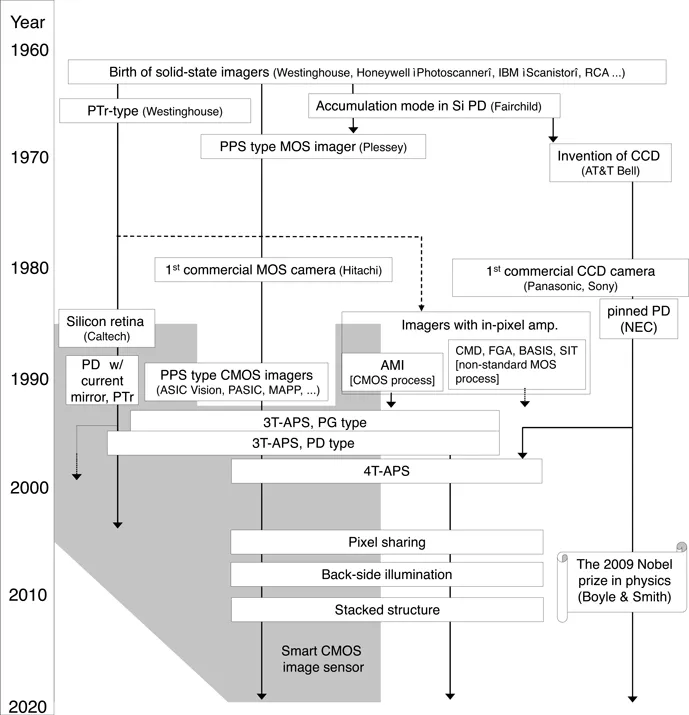
Revised and expanded for this new edition, Smart CMOS Image Sensors and Applications, Second Edition is the only book available devoted to smart CMOS image sensors and applications. The book describes the fundamentals of CMOS image sensors and optoelectronic device physics, and introduces typical CMOS image sensor structures, such as the active pixel sensor (APS). Also included are the functions and materials of smart CMOS image sensors and present examples of smart imaging. Various applications of smart CMOS image sensors are also discussed. Several appendices supply a range of information on constants, illuminance, MOSFET characteristics, and optical resolution. Expansion of smart materials, smart imaging and applications, including biotechnology and optical wireless communication, are included.
Features
⢠Covers the fundamentals and applications including smart materials, smart imaging, and various applications
⢠Includes comprehensive references
⢠Discusses a wide variety of applications of smart CMOS image sensors including biotechnology and optical wireless communication
⢠Revised and expanded to include the state of the art of smart image sensors
Frequently asked questions
Yes, you can cancel anytime from the Subscription tab in your account settings on the Perlego website. Your subscription will stay active until the end of your current billing period. Learn how to cancel your subscription.
No, books cannot be downloaded as external files, such as PDFs, for use outside of Perlego. However, you can download books within the Perlego app for offline reading on mobile or tablet. Learn more here.
Perlego offers two plans: Essential and Complete
Essential is ideal for learners and professionals who enjoy exploring a wide range of subjects. Access the Essential Library with 800,000+ trusted titles and best-sellers across business, personal growth, and the humanities. Includes unlimited reading time and Standard Read Aloud voice.
Complete: Perfect for advanced learners and researchers needing full, unrestricted access. Unlock 1.4M+ books across hundreds of subjects, including academic and specialized titles. The Complete Plan also includes advanced features like Premium Read Aloud and Research Assistant.
Both plans are available with monthly, semester, or annual billing cycles.
We are an online textbook subscription service, where you can get access to an entire online library for less than the price of a single book per month. With over 1 million books across 1000+ topics, weāve got you covered! Learn more here.
Look out for the read-aloud symbol on your next book to see if you can listen to it. The read-aloud tool reads text aloud for you, highlighting the text as it is being read. You can pause it, speed it up and slow it down. Learn more here.
Yes! You can use the Perlego app on both iOS or Android devices to read anytime, anywhere ā even offline. Perfect for commutes or when youāre on the go. Please note we cannot support devices running on iOS 13 and Android 7 or earlier. Learn more about using the app.
Yes, you can access Smart CMOS Image Sensors and Applications by Jun Ohta in PDF and/or ePUB format, as well as other popular books in Technology & Engineering & Electrical Engineering & Telecommunications. We have over one million books available in our catalogue for you to explore.
Complementary metal-oxide-semiconductor (CMOS) image sensors have been the subject of extensive research and development and currently surpass the market with charge coupled device (CCD) image sensors, which have dominated the field of imaging sensors for a long time. CMOS image sensors are now widely used not only for consumer electronics, such as compact digital still cameras (DSC), mobile phone cameras, handy-camcorders, and digital single lens reflex (DSLR) cameras, but also for cameras used in automobiles, surveillance, security, robot vision, etc. Recently, further applications of CMOS image sensors in biotechnology and medicine have emerged. Many of these applications require advanced performance features, such as wide dynamic range, high speed, and high sensitivity, while others need dedicated functions, for example, three-dimensional (3D) range finding. It is difficult to perform such tasks with conventional image sensors. Furthermore, some signal processing devices are insufficient for these purposes. Smart CMOS image sensors or CMOS image sensors with integrated smart functions on the chip may meet the requirements of these applications.
CMOS image sensors are fabricated based on standard CMOS large scale integration (LSI) fabrication processes, while CCD image sensors are based on a specially developed fabrication process. This feature of CMOS image sensors makes it possible to integrate the functional circuits to develop smart CMOS image sensors and that can realize not only a higher performance than that of the CCD and conventional CMOS image sensors, but also perform versatile functions that cannot be achieved with conventional image sensors.
Smart CMOS image sensors are mainly aimed at two objectives: (i) enhancing or improving the fundamental characteristics of CMOS image sensors, such as dynamic range, speed, and sensitivity; (ii) implementing new functions, such as 3D range finding and modulated light detection. For both objectives, many architectures and/or structures, as well as materials, have been proposed and demonstrated.
The following terms are also associated with smart CMOS image sensors: computational CMOS image sensors, integrated functional CMOS image sensors, vision chips, focal plane image processing, as well as many others. With the exception of vision chips, these terms suggest that an image sensor has other functions in addition to imaging. The name vision chip originates from a device proposed and developed by C. Mead and coworkers, which mimics the human visual processing system. This topic will be described later in this chapter. In the following section, we first present a survey of the history of CMOS image sensors in general, and then briefly review the history of smart CMOS image sensors, in particular. For a summarized history of various imagers, including the CCDs, the readers are advised to refer to Ref. [10].
1.2Brief history of CMOS image sensors
Birth of MOS imagers
The history of MOS image sensors, shown in Fig. 1.1, started with solid-sate imagers used as a replacement for image tubes. For solid-state image sensors, four important functions had to be realized: light-detection, accumulation of photo-generated signals, switching from accumulation to readout, and scanning. These functions are discussed in Chapter 2. The scanning function in XāY addressed silicon-junction photosensing devices was proposed in the early 1960s by S.R. Morrison at Honeywell as the āphotoscannerā [11] and by J.W. Horton et al. at IBM as the āscanistorā [12]. P.K. Weimer et al. proposed solid-state image sensors with scanning circuits using thin-film transistors (TFTs) [13]. In these devices, photo-conductive film, discussed in Sec. 2.3.5, is used for the photo-detector. M.A. Schuster and G. Strull at NASA used photo-transistors (PTrs) as photo-detectors, as well as switching devices to realize XāY addressing [14]. They successfully obtained images with a fabricated 50 Ć 50-pixel array sensor. PTrs are discussed in Sec. 2.3.3.
FIGURE 1.1: Evolution of MOS image sensors and related inventions.
The accumulation mode in a photodiode is an important function for MOS image sensors and is described in Sec. 2.4. It was first proposed by G.P. Weckler at Fairchild Semiconductor [15]. In the proposal, the floating source of a metalāoxideāsemiconductor filedāeffect transistor (MOSFET) was used as a photodiode. This structure is used in some present CMOS image sensors. Weckler later fabricated and demonstrated a 100 Ć 100-pixel image sensor using this structure [16]. Since then, several types of solid-sate image sensors have been proposed and developed [16ā19], as summarized in Ref. [20].
The solid-state image sensor developed by P.J. Noble at Plessey was almost the same as the MOS image sensor or passive pixel sensor (PPS), discussed in Sec. 2.5.1, consisting of a photodiode and a switching MOS transistor in a pixel with X- and Y-scanners and a charge amplifier. Noble briefly discussed the possibility of integrating logic circuitry for pattern recognition on a chip, which may be the first prediction of a smart CMOS image sensor.
1.2.1Competition with CCDs
Shortly after the publication of the details of solid-state image sensors in IEEE Transactions on Electron Devices in 1968, the CCD image sensors become prominent [21]. The CCD itself was invented in 1969 by W. Boyle and G.E. Smith at AT&T Bell Laboratories [21] and was experimentally verified at almost the same time [22]. Initially, the CDD was developed as semiconductor memory, and as a replacement for magnetic bubble memory; however, it was soon developed for use in image sensors, which was invented by Michael F. Tompsett [23]. The early stage of the invention of the CCD is described in Ref. [24].
Considerable research effort resulted in the production of the first commercial MOS imagers, appearing in the 1980s [25ā30]. While Hitachi had developed MOS imagers [25, 27], until recently only the CCDs were widely manufactured and used as they offered superior image quality than MOS imagers.
1.2.2Solid-state imagers with in-pixel amplification
Subsequently, efforts were made to improve the signal-to-noise ratio (SNR) of MOS imagers by incorporating an amplification mechanism in a pixel. In the 1960s, a photo-transistor (PTr) type imager was developed [14]. In the late 1980s, several amplifier type imagers were developed, including the charge modulated device (CMD) [31], floating gate array (FGA) [32], base-stored image sensor (BASIS) [33], static induction transistor (SIT) [34], amplified MOS imager (AMI) [35ā39], and some others [6, 7]. Apart from the AMI, these required some modification of standard MOS fabrication technology in the pixel structure. Ultimately they were not commercialized and their development was terminated. The AMI can be fabricated using the standard CMOS technology without any modification; however, its pixel structure is the same as that of the active pixel sensor (APS). It should be noted that the AMI uses an IāV converter as a readout circuit while the APS uses a source follower, even though this difference is not critical. The APS is also classified as an image sensor with in-pixel amplification.
1.2.3Present CMOS image sensors
The APS was first realized by using a photogate (PG) as a photo-detector by E. Fossum et al. at JPL* and then by using a photodiode (PD) [40, 41]. A PG was used owing mainly to the ease of signal charge handling. The sensitivity of a PG is not adequate as poly-silicon as a gate material is opaque in the visible wavelength region. APSs using a PD are called 3T-APSs (three transistor APSs) and are now widely used in CMOS image sensors. In the first stage of 3T-APS development, the image quality could not compete with that of CCDs, both with respect to fixed pattern noise (FPN) and random noise. Introducing noise canceling circuits reduces...