Recently the world celebrated the 60th anniversary of the invention of the first transistor. The first integrated circuit (IC) was built a decade later, with the first microprocessor designed in the early 1970s. Today, ICs are a part of nearly every aspect of our daily lives. They help us live longer and more comfortably, and do more, faster. All this is possible because of the relentless search for new materials, circuit designs, and ideas happening on a daily basis at industrial and academic institutions around the globe.
Showcasing the latest advances in very-large-scale integrated (VLSI) circuits, VLSI: Circuits for Emerging Applications provides a balanced view of industrial and academic developments beyond silicon and complementary metal–oxide–semiconductor (CMOS) technology. From quantum-dot cellular automata (QCA) to chips for cochlear implants, this must-have resource:
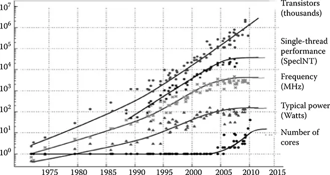
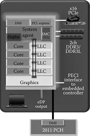
- Investigates the trend of combining multiple cores in a single chip to boost performance of the overall system
- Describes a novel approach to enable physically unclonable functions (PUFs) using intrinsic features of a VLSI chip
- Examines the VLSI implementations of major symmetric and asymmetric key cryptographic algorithms, hash functions, and digital signatures
- Discusses nonvolatile memories such as resistive random-access memory (Re-RAM), magneto-resistive RAM (MRAM), and floating-body RAM (FB-RAM)
- Explores organic transistors, soft errors, photonics, nanoelectromechanical (NEM) relays, reversible computation, bioinformatics, asynchronous logic, and more
VLSI: Circuits for Emerging Applications presents cutting-edge research, design architectures, materials, and uses for VLSI circuits, offering valuable insight into the current state of the art of micro- and nanoelectronics.