
- 920 pages
- English
- ePUB (mobile friendly)
- Available on iOS & Android
eBook - ePub
About this book
Emphasizing the detailed design of various Verilog projects, Verilog HDL: Digital Design and Modeling offers students a firm foundation on the subject matter. The textbook presents the complete Verilog language by describing different modeling constructs supported by Verilog and by providing numerous design examples and problems in each chapter. Examples include counters of different moduli, half adders, full adders, a carry lookahead adder, array multipliers, different types of Moore and Mealy machines, and much more. The text also contains information on synchronous and asynchronous sequential machines, including pulse-mode asynchronous sequential machines.
In addition, it provides descriptions of the design module, the test bench module, the outputs obtained from the simulator, and the waveforms obtained from the simulator illustrating the complete functional operation of the design. Where applicable, a detailed review of the topic's theory is presented together with logic design principles, including state diagrams, Karnaugh maps, equations, and the logic diagram.
Verilog HDL: Digital Design and Modeling is a comprehensive, self-contained, and inclusive textbook that carries all designs through to completion, preparing students to thoroughly understand this popular hardware description language.
Trusted by 375,005 students
Access to over 1.5 million titles for a fair monthly price.
Study more efficiently using our study tools.
Information
1
Introduction
1.1 History of HDL
1.2 Verilog HDL
1.3 Assertion Levels
This book covers the design of combinational and sequential logic using the Verilog hardware description language (HDL). An HDL is a method of designing digital hardware by means of software. A considerable saving of time can be realized when designing systems using an HDL. This offers a competitive advantage by reducing the time-to-market for a system. Another advantage is that the design can be simulated and tested for correct functional operation before implementing the system in hardware. Any errors that are found during simulation can be corrected before committing the design to expensive hardware implementation.
1.1 History of HDL
HDLs became popular in the 1980s and were used to describe large digital systems using a textual format rather than a schematic format such as logic diagrams. With the advent of application-specific integrated circuits (ASICs), field programmable gate arrays (FPGAs), and complex programmable logic devices (CPLDs), computer-aided engineering techniques became necessary. This allowed the engineers to use a programming language to design the logic of the system. Using this technique, test benches could be designed to simulate the entire system and obtain binary outputs and waveforms. Many of these languages were proprietary and not placed in the public domain. Verilog HDL is one of two primary hardware description languages. The other main HDL is the Very High Speed Integrated Circuit (VHSIC) hardware description language (VHDL). VHDL was developed for the United States Department of Defense and was created jointly by IBM, Texas Instruments, and Intermetrics. Although VHDL has not achieved the widespread acceptance of Verilog, both are IEEE standards.
HDLs allow the designer to easily and quickly express architectural concepts in a precise notation without the aid of logic diagrams. All HDLs express the same fundamental concepts, but in slightly different notations.
1.2 Verilog HDL
The Verilog hardware description language is the state-of-the-art method for designing digital and computer systems. Verilog HDL is a C-like language — with some Pascal syntax — used to model a digital system at many levels of abstraction from a logic gate to a complex digital system to a mainframe computer. The combination of C and Pascal syntax makes Verilog easy to learn. The completed design is then simulated to verify correct functional operation. Verilog HDL is the most widely used HDL in the industry.
The Verilog HDL is able to describe both combinational and sequential logic, including level-sensitive and edge-triggered storage devices. Verilog provides a clear relationship between the language syntax and the physical hardware.
The Verilog simulator used in this book is easy to learn and use, yet powerful enough for any application. It is a logic simulator — called SILOS — developed by Silvaco International for use in the design and verification of digital systems. The SILOS simulation environment is a method to quickly prototype and debug any ASIC, FPGA, or CPLD design. It is an intuitive environment that displays every variable and port from a module to a logic gate. SILOS allows single stepping through the Verilog source code, as well as drag-and-drop ability from the source code to a data analyzer for waveform generation and analysis.
Verilog HDL supports a top-down design approach of hierarchical decomposition as well as a bottom-up approach. In a top-down design method, the top-level block is defined, then each sub-block that is used to build the top-level is defined. These second-level blocks are then further subdivided until the lowest level is defined. In a bottom-up method, the building blocks (modules) are first defined. These modules are then used to build larger modules, which are then instantiated into a structural module. Verilog can be used to model algorithms, Boolean equations, and individual logic gates. Simulation occurs at different levels. The low-level modules are first designed and tested for correct functional operation by the simulator using a test bench. These modules are then instantiated into the top-level (structural) module, which is then simulated by means of a test bench.
1.2.1 IEEE Standard
Verilog HDL was developed by Phillip Moorby in 1984 as a proprietary HDL for Gateway Design Automation. Gateway was later acquired by Cadence Design Systems, which placed the language in the public domain in 1990. The Open Verilog International was then formed to promote the Verilog HDL language. In 1995, Verilog was made an IEEE standard HDL (IEEE Standard 1364-1995) and is described in the Verilog Hardware Description Language Reference Manual.
1.2.2 Features
Logic primitives such as AND, OR, NAND, and NOR gates are part of the Verilog language. These are built-in primitives that can be instantiated into a module. The designer also has the option of creating a user-defined primitive (UDP), which can then be instantiated into a module in the same way as a built-in primitive. UDPs can be any logic function such as a multiplexer, decoder, encoder, or flip-flop.
Different types of delays can be introduced into a logic circuit including: interstatement, intrastatement, inertial, and transport delays. These will be defined later in the appropriate sections.
Designs can be modeled in three different modeling constructs: (1) dataflow, (2) behavioral, and (3) structural. Module design can also be done in a mixed-design style, which incorporates the above constructs as well as built-in and user-defined primitives. Structural modeling can be described for any number of module instantiations.
Verilog does not impose a limit to the size of the system; therefore, SILOS can be used to design any size system. Verilog can be used not only to design all the modules of a system, but also to design the test bench that is used for simulation.
Verilog also has available bitwise logic functions such as bitwise AND (&) and bitwise OR ( | ). High-level programming language constructs such as multiway branching (case statements), conditional statements, and loops are also available.
1.3 Assertion Levels
There are different ways to indicate the active level (or assertion) of a signal. Table 1.1 lists various methods used by companies and textbooks. This book will use the +A and –A method. The AND function can be represented three ways, as shown in Figure 1.1, using an AND gate, a NAND gate, and a NOR gate. Although only two inputs are shown, both AND and OR circuits can have three or more inputs. The plus (+) and minus (–) symbols that are placed to the left of the variables indicate a high or low voltage level, respectively. This indicates the asserted (or active) voltage level for the variables; that is, the logical 1 (or true) state, in contrast to the logical 0 (or false) state.
Table 1.1 Assertion Levels

Thus, a signal can be asserted either plus or minus, depending upon the active condition of the signal at that point. For example, Figure 1.1(a) specifies that the AND function will be realized when both input A and input B are at their more positive potential, thus generating an output at its more positive potential. The word positive as used here does not necessarily mean a positive voltage level, but merely the more positive of two voltage levels. Therefore, the output of the AND gate of Figure 1.1(a) can be written as + (A & B).
To illustrate that a plus level does not necessarily mean a positive voltage level, consider two logic families: transistor-transistor logic (TTL) and emitter-coupled logic (ECL). The TTL family uses a + 5 volt power supply. A plus level is approximately + 3.5 volts and above; a minus level is approximately + 0.2 volts. The ECL family uses a – 5.2 volt power supply. A plus level is approximately – 0.95 volts; a minus level is approximately – 1.7 volts. Although – 0.95 volts is a negative voltage, it is the more positive of the two ECL voltages.
The logic symbol of Figure 1.1(b) is a NAND gate in which inputs A and B must both be at their more positive potential for the output to be at its more negative potential. A small circle (or wedge symbol for IEEE std 91-1984 logic functions) at the input or output of a logic gate indicates a more negative potential. The output of the NAND gate can be written as – (A & B).
Figure 1.1(c) illustrates a NOR gate used for the AND function. In this case, inputs A and B must be active (or asserted) at their more negative potential in order for the output to be at its more positive potential. The output can be written as + (A & B). A variable can be active (or asserted) at a high and a low level at the same time, as shown in Figure 1.2.
Figure 1.1(d) shows a NAND gate used for the OR function. Either input A or B (or both) must be at its more negative potential to assert the output at its more positive potential. The output can be written as + (A | B), where the symbol ( | ) indicates the OR operation in Verilog.
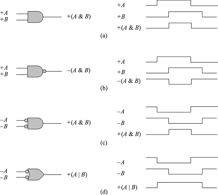
Figure 1.1 Logic symbols and waveforms for AND, NAND, NOR, and NAND (negative-input OR).
Figure 1.2 Signals can be active high and low at the same time.
2
Overview
2.1 Design Methodologies
2.2 Modulo-16 Synchronous Counter
2.3 Four-Bit Ripple Adder
2.4 Modules and Ports
2.5 Introduction to Dataflow Modeling
2.6 Introduction ...
Table of contents
- Cover
- Half Title
- Title Page
- Copyright Page
- Dedication Page
- Table of Contents
- Preface
- Chapter 1 Introduction
- Chapter 2 Overview
- Chapter 3 Language Elements
- Chapter 4 Expressions
- Chapter 5 Gate-Level Modeling
- Chapter 6 User-Defined Primitives
- Chapter 7 Dataflow Modeling
- Chapter 8 Behavioral Modeling
- Chapter 9 Structural Modeling
- Chapter 10 Tasks and Functions
- Chapter 11 Additional Design Examples
- Appendix A Event Queue
- Appendix B Verilog Project Procedure
- Appendix C Answers to Select Problems
- Index
Frequently asked questions
Yes, you can cancel anytime from the Subscription tab in your account settings on the Perlego website. Your subscription will stay active until the end of your current billing period. Learn how to cancel your subscription
No, books cannot be downloaded as external files, such as PDFs, for use outside of Perlego. However, you can download books within the Perlego app for offline reading on mobile or tablet. Learn how to download books offline
Perlego offers two plans: Essential and Complete
- Essential is ideal for learners and professionals who enjoy exploring a wide range of subjects. Access the Essential Library with 800,000+ trusted titles and best-sellers across business, personal growth, and the humanities. Includes unlimited reading time and Standard Read Aloud voice.
- Complete: Perfect for advanced learners and researchers needing full, unrestricted access. Unlock 1.5M+ books across hundreds of subjects, including academic and specialized titles. The Complete Plan also includes advanced features like Premium Read Aloud and Research Assistant.
We are an online textbook subscription service, where you can get access to an entire online library for less than the price of a single book per month. With over 1.5 million books across 990+ topics, we’ve got you covered! Learn about our mission
Look out for the read-aloud symbol on your next book to see if you can listen to it. The read-aloud tool reads text aloud for you, highlighting the text as it is being read. You can pause it, speed it up and slow it down. Learn more about Read Aloud
Yes! You can use the Perlego app on both iOS and Android devices to read anytime, anywhere — even offline. Perfect for commutes or when you’re on the go.
Please note we cannot support devices running on iOS 13 and Android 7 or earlier. Learn more about using the app
Please note we cannot support devices running on iOS 13 and Android 7 or earlier. Learn more about using the app
Yes, you can access Verilog HDL by Joseph Cavanagh in PDF and/or ePUB format, as well as other popular books in Technology & Engineering & Computer Engineering. We have over 1.5 million books available in our catalogue for you to explore.