![]()
Part I
CMOS Technology at the Nanoscale
![]()
1 CMOS: An Emerging Technology System Driver
Paul Rousseau
CONTENTS
1.1 CMOS Rise to Dominance: A Very Brief History
1.2 CMOS Is Everywhere
1.3 Logic-Based Embedded DRAM CMOS
1.4 Logic-Based Embedded Flash CMOS
1.5 High-Voltage CMOS
1.6 CMOS Image Sensor
1.7 RF CMOS and SiGe BiCMOS
1.8 Other Technology Considerations
1.8.1 Automotive
1.8.2 MEMS
1.8.3 SoC versus SiP
1.9 Conclusions
References
1.1 CMOS RISE TO DOMINANCE: A VERY BRIEF HISTORY
This is not a real history of complementary metal oxide semiconductor (CMOS), but rather a rapid overview of the steps in getting to CMOS. Whereas key inventions are important, their applications to manufacturing are really the milestones in this march. For example, although the field-effect transistor (FET) may have been the first proposed in the 1930s, it could not be built. The first transistor honors and the Nobel Prize went to the bipolar device. Whereas the 1960s was the decade of the bipolar, the early 1970s saw the introduction of P-channel metal oxide semiconductor (PMOS) followed by the higher performance N-channel mixed oxide semiconductor (NMOS) in the late 1970s. By the 1980s, CMOS was establishing itself as the technology of the future and by the 1990s, unquestionably CMOS was the king of logic, a position it has only strengthened today.
Several factors contributed to this rise. First and foremost, the low standby power that CMOS offered as originally proposed by Wanlass of Fairchild in 1963 [1]. Second, the ability to scale MOS efficiently as articulated by Dennard et al. of IBM [2]. Third, the simple fact that an affordable and manufacturable process could be developed for CMOS.
Today, as CMOS gate oxide scales to dimensions between 10 and 15 Å and gate leakage approaches that of a bipolar base, there is still no turning back. As a voltage-controlled current device, CMOS is ideally suited as a low standby power circuit. It is much harder to imagine this property with bipolar, as it is a current-controlled device. Some may argue that this distinction is arbitrary as one can consider base–emitter voltage (Vbe) as a voltage control. But can I have Vbe high (0.6–0.9 V range) without significant current? No, yet in CMOS, I can have high gate-source voltage (Vgs) and still have no current flow.
Still, there are clouds on the horizon. As gate leakage and source drain leakage became too important, the scaling laws were abandoned. The power supply voltage has stopped scaling, and the power reductions afforded by such scaling were lost. The power problem grew, implying that designers needed to add power closure on top of the timing closure.
Nevertheless, human ingenuity has kept going and as CMOS marches down the scaling curve, the focus has been to keep tweaking it, even when this involves fairly fundamental structural changes. Strained silicon was introduced to improve performance, and scaling continued in its modified way, still helping reduce the power problem. Perhaps most dramatic has been the recent introduction of high-k metal gate (HKMG) as reported by Intel [3], a complete reengineering of the very heart of the transistor. This solves the gate leakage problem, as least for now.
Process and design have to work hand in hand. Multithresholds methodologies have become very common. Multivoltage domains, dynamic voltage scaling, and sleep mode back biasing methodologies were also introduced to manage the power, although always at the cost of additional complexity.
Whereas these problems left the door open for a contender to CMOS, the task is formidable. For example, electron spin device make interesting scientific papers, but how do we connect a million of them, let alone a billion together to produce a useful system? The beauty of transistors is they react to charge and so to connect one transistor to the next, I just need a wire, thus allowing charge transfer. And, as we shall see, wires are very cheap. How can I do this for spin devices?
Still, there are potential viable candidates waiting for their chance. Fundamentally, the MOS device is flawed by the fact that once in inversion, the current drive increases linearly with supply voltage (this holds for deep submicron device in velocity saturation mode). The device of the future will need an exponential turn on, similar to emitter-coupled logic (ECL) and this will allow scaling of the power supply voltage, hence the power. But that is the potential for future, for now, CMOS reigns supreme.
1.2 CMOS IS EVERYWHERE
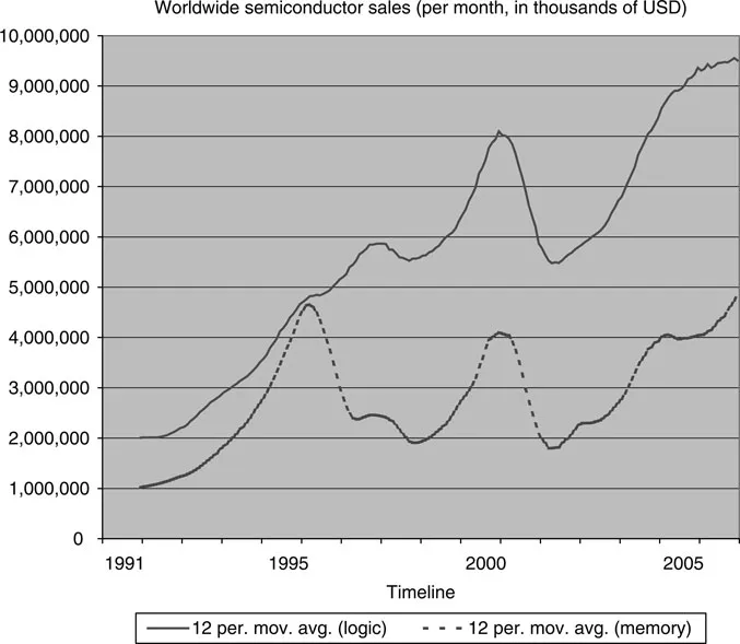
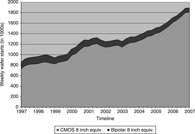
Worldwide monthly semiconductor sales from 1991 through 2006 are shown in Figure 1.1. Although memory almost caught up with logic in 1996, the data shows the clear dominance of logic wafers, more than two times bigger than the memory sales. Within logic, Figure 1.2 shows wafer starts from 1997 to 2007. The data illustrate the dominance of CMOS logic over bipolar that only keeps growing, from ~90% of wafer starts in 1997 to ~95% of wafer starts in 2007. The total numbers are also very significant. With over $200 billion in logic wafer sales, it is clear that this supports a significant R&D effort and capital expenditure that nothing else can compete with. Therefore the semiconductor processing tools are focused on CMOS logic and the foundries, the integrated device manufacturers (IDMs) are focused on CMOS logic as well as the design tool providers and the intellectual property (IP) industry. Basically the sheer size of CMOS logic means that an entire and well-oiled ecosystem has been built on supporting CMOS logic first and making it the technology driver.
One reason for CMOS success has been cost. Scaling, as described by Moore’s observation, has doubled the density with each generation, with the associated cost reduction. Applications such as graphical processing unit (GPU), which are “Moore law–friendly,” can take full advantage of these benefits. Nvidia is a good case in point; they have maintained close to 2× doubling of transistor count every year [4].
In 65 nm technology, $1 can purchase well over 10 million transistors. What can you accomplish with 10 million transistors? How about with 1 billion; this is within reach now. And this cost includes eight levels of copper wiring to interconnect these transistors together, meaning each wire costs a fraction of a microcent.
Now that we have seen that logic is the 800 lb gorilla in the room, and memory is the 300 lb chimpanzee, it is instructive to further explore how these differ in what they enable. There is no question that memory has been a separate technology driver and its products can enable whole new systems; one only has to think of the explosion of digital photography, or portable digital music in recent years. However, memory remains a somewhat standardized and therefore commoditized market, dominated by a few large manufacturers in flash and dynamic random access memory (DRAM). The reasons behind this are fairly straightforward. Although I can enable interesting new systems with memory, it is hard to build memory chips with new functions. Higher density, speed, lower power consumption are the standard fare of memory scaling. In fact, memory technologies are so poor at implementating logic functions that there is a proliferation of logics chip that, built into multichip module (MCM) with memory, aid in optimizing this memory.
FIGURE 1.1 Worldwide semiconductor sales by month from 1991 to 2006 using 12-month moving average to remove seasonal variations.
FIGURE 1.2 Weekly logic wafer production from 1997 to 2007 by quarters in 8 in. equivalents (Semiconductor Industry Association data).
Logic on the other hand is the Lego set of designers. Given a logic process with appropriate design tools and technology files, designers have endless possibilities as to how to connect these transistors together to perform new and useful functions. Eventhough for advanced logic, the standard metrics of higher density, faster, lower power still hold, we have not finished exploiting the potential of older technologies and really the only limiting factor is ...