![]()
Part I
Contact Interface Conduction
![]()
1
Electrical Contact Resistance: Fundamental Principles
Roland S. Timsit
Only connect!
Howards End, E M Forster
CONTENTS
1.1 Introduction
1.2 Electrical Constriction Resistance
1.2.1 Circular a-spots
1.2.2 Non-Circular and Ring a-Spots
1.2.3 Multiple Contact Spots
1.2.4 Effect of the Shape of Contact Asperity on Constriction Resistance
1.3 Effect of Surface Films on Constriction and Contact Resistance
1.3.1 Electrically Conductive Layers on an Insulated Substrate
1.3.1.1 Calculation of Spreading Resistance in a Thin Film
1.3.2 Electrically Conducting Layers on a Conducting Substrate
1.3.2.1 Electrically Conducting Layers and Thin Contaminant Films
1.3.3 Growth of Intermetallic Layers
1.3.4 Possible Effect of Electromigration on Intermetallic Growth Rates
1.3.5 Electrically Insulating or Weakly Conducting Films
1.3.5.1 Growth Rate and Electrical Resistivity of Oxides of Selected Contact Materials
1.3.6 Fritting of Electrically Insulating Surface Films
1.4 Temperature of an Electrically Heated a-Spot
1.4.1 Voltage–Temperature Relation
1.4.2 Voltage–Temperature Relation with Temperature–Dependent Electrical Resistivity and Thermal Conductivity
1.4.3 The Wiedemann–Franz Law
1.4.4 Temperature Distribution in the Vicinity of an a-Spot
1.4.5 Deviation of the Voltage–Temperature Relation in an Assymetric Contact
1.4.5.1 Case I: Two Metals in Contact
1.4.5.2 Case II: A Metal in Contact with a Non-metal
1.4.6 Special Considerations on the “Melting” Voltage in Electrical Contacts
1.5 Mechanics of a-Spot Formation
1.5.1 Smooth Interfaces
1.5.2 Rough Interfaces
1.6 Breakdown of Classical Electrical Contact Theory in Small Contact Spots
1.6.1 Electrical Conduction in Small a-Spots
1.6.1.1 Contact Resistance
1.6.1.2 Joule Heat Flow Through a-Spots
1.6.2 Observations of Breakdown of Classical Electrical Contact Theory in Aluminum Contacts
1.6.2.1 Experimental Data on Aluminum
1.6.3 Observations of Breakdown of Classical Electrical Contact Theory in Gold Contacts
1.6.4 Observations of Breakdown of Classical Electrical Contact Theory in Tin Contacts
1.7 Constriction Resistance at High Frequencies
1.7.1 Skin Depth and Constriction Resistance
1.7.2 Evaluation of Constriction Resistance at High Frequencies
1.7.3 Constriction versus Connection Resistance at High Frequencies
1.8 Summary
Acknowledgments
References
1.1 Introduction
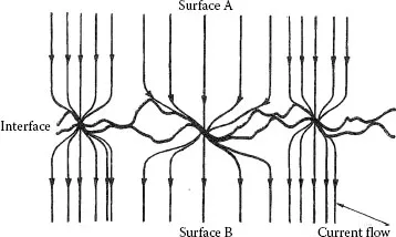
All solid surfaces are rough on the microscale. Surface microroughness consists of peaks and troughs whose shape, variations in height, average separation, and other geometrical characteristics depend on fine details of the surface generation process [1]. Contact between two engineering bodies, thus, occurs at discrete spots produced by the mechanical contact of asperities on the two surfaces, as illustrated in Figure 1.1. For all solid materials, the area of true contact is, thus, a small fraction of the nominal contact area, for a wide range of contact loads [1,2]. The mode of deformation of contacting asperities is either elastic, plastic, or mixed elastic–plastic depending on local mechanical contact stresses and on properties of the materials, such as elastic modulus and hardness. In a bulk electrical interface where the mating components are metals, the contacting surfaces are often covered with oxide or other electrically insulating layers. Generally, the interface becomes electrically conductive only when metal-to-metal contact spots are produced, that is, where electrically insulating films are ruptured or displaced at the asperities of the contacting surfaces. In a typical bulk electrical junction, the area of electrical contact is, thus, appreciably smaller than the area of true mechanical contact.
In a bulk electrical junction, the electric current lines become increasingly distorted as the contact interface is approached and the flow lines bundle together to pass through the separate contact spots (or “a-spots"), as illustrated in Figure 1.1. Constriction of the electric current by a-spots reduces the volume of material used for electrical conduction and thus increases electrical resistance. This increase in resistance is defined as the constriction resistance of the interface. Often, the presence of contaminant films of relatively large electrical resistivity on the contacting surfaces increases the resistance of a-spots beyond the value given by constriction resistance. The total interfacing resistance provided by the constriction and film resistances determines the contact resistance of the interface.
FIGURE 1.1
Schematic diagram of a bulk electrical interface.
The present chapter reviews some fundamental properties of electrical contacts and updates the reader on the results of recent research. The review focuses on the effect of constriction of current flow on electrical resistance, interdiffusion processes at electrical interfaces, the relationship between the drop in electrical potential and temperature in an electrical contact (the so-called voltage–temperature relation), sintering, softening, and melting in contact spots, the effect of deformation...