![]()
1
Clock Generation and Distribution for Low-Power Digital Systems
Martin Cochet, Guénolé Lallement, Fady Abouzeid, and Philippe Roche
CONTENTS
1.1Introduction
1.2Different Levels of Timekeeping
1.3Time References
1.3.1Design Considerations in IoT Nodes: Power, Area, and Stability
1.3.2Fundamental Frequency and Time Metrology
1.3.3Evaluation of Low-Power Time References
1.4Frequency Multipliers
1.4.1Clock Multiplier Metrics
1.4.2Low-Power PLLs
1.4.3Alternatives to PLLs
1.5Clock Distribution
1.6Conclusion
A.1Appendix: Quantitative Definitions of Jitter
A.1.1Long-Term Jitter: Frequency Domain Analysis
A.1.2Period Jitter
A.1.3Quantifying the Impact of Jitter on Power Budget
References
1.1 Introduction
Digital circuits and systems have been a part of modern life for more than 40 years, whether in the form of digital signal processors, processors, or application-specific integrated circuits. All these systems rely on efficient flexible clock generation as well as distribution to pace their functionality and have some requirement in that process: the clock signal must be produced accurately (i.e., with a low jitter value), its frequency must be tunable to achieve different processing speeds and power trade-off, and the whole generation and distribution process must have a limited area and power overhead at the system level.
The last decade has seen a rise in low-power digital systems, from embedded mobile processors to Internet of Things (IoT) applications. When considering these systems, the previously described clock delivery constraints still exist partially, while some are alleviated and other problems arise.
The considered systems operate down to near-threshold voltages (0.4–0.6 V) and low frequencies (1-50 MHz) to fit within highly constrained power budgets (in the microwatt to milliwatt range). This translates to different clocking constraints: the absolute accuracy, often quantified as jitter in picosecond, is less critical over a longer clock period. Yet the power overhead of all parts of the clock chain must be compared to a much lower total power budget. This requires specific redesign strategies of the full clock chain. Last, low-voltage operation introduces increased variability and standard cell balancing issues that have to be accounted for.
This chapter describes the design strategies elaborated along the clock chain. The first section describes the typical topology of a low-power microcontroller system and introduces the clocking requirements. The second section introduces the reference clock sources. The third section presents frequency multiplier strategies, and the last section covers distribution through clock trees.
1.2 Different Levels of Timekeeping
This section focuses on the most power-constrained digital systems, for IoT applications. These systems assume different detailed architectures depending on their use cases, which range from miniaturized implantable biomedical sensors [1] to industrial machine diagnosis application [2], or the most commonly known personal IoT [3,4].
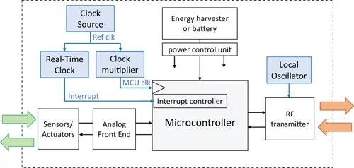
However different, these systems share a common structure, as illustrated in Figure 1.1. The system interacts with the physical world through sensors and actuators interfaced via an analog front end. Then, the data are processed by a microcontroller unit (MCU), or full processor, before being transmitted to a base station via a radiofrequency (RF) interface. The whole system is powered by a battery and/or the output of an energy harvester.
The different clock sources are shown in blue in Figure 1.1. First, an absolute time reference has to be generated, typically through a quartz on board, though on-chip integrated solutions are now proposed. This reference has a low frequency, with a standard of 32.768 kHz.1 This reference has two roles. First, it is used by the real-time clock (RTC) circuit, which acts as a counter to generate timed interrupt commands to the MCU. These are used to either acquire or transmit data at fixed intervals. Second, the same time reference can be used as an input to generate the main MCU clock. Depending on the application, that clock will operate from a couple to several hundred megahertz. A clock multiplier circuit is used to generate that signal. It is composed of an oscillator whose frequency is tuned to match a multiple of the reference. The most common architecture is a phase-locked loop (PLL), but other topologies will be presented in Section 1.4. Last, the RF transmitter uses a high-frequency local oscillator (e.g., 2.4GHz for bluetooth). The specifications for this clock source are very different from the digital ones, and rely on different power management strategies, depending on the RF application, such as wake-up receivers [5], and are beyond the scope of this chapter.
FIGURE 1.1
Generic block di...