- 512 pages
- English
- ePUB (mobile friendly)
- Available on iOS & Android
eBook - ePub
Analog Circuits and Devices
About this book
The Principles and Application in Engineering Series is a new series of convenient, economical references sharply focused on particular engineering topics and subspecialties. Each volume in this series comprises chapters carefully selected from CRC's bestselling handbooks, logically organized for optimum convenience, and thoughtfully priced to fit
Trusted by 375,005 students
Access to over 1.5 million titles for a fair monthly price.
Study more efficiently using our study tools.
Information
1
Bipolar Junction Transistor (BJT) Circuits
David J.Comer
Donald T.Comer
Brigham Young University
1.1 Introduction
The bipolar junction transistor (or BJT) was the workhorse of the electronics industry from the 1950s through the 1990s. This device was responsible for enabling the computer age as well as the modern era of communications. Although early systems that demonstrated the feasibility of electronic computers used the vacuum tube, the element was too unreliable for dependable, long-lasting computers. The invention of the BJT in 19471 and the rapid improvement in this device led to the development of highly reliable electronic computers and modern communication systems.
Integrated circuits, based on the BJT, became commercially available in the mid- 1960s and further improved the dependability of the computer and other electronic systems while reducing the size and cost of the overall system. Ultimately, the microprocessor chip was developed in the early 1970s and the age of small, capable, personal computers was ushered in. While the metal-oxide-semiconductor (or MOS) device is now more prominent than the BJT in the personal computer arena, the BJT is still important in larger high-speed computers. This device also continues to be important in communication systems and power control systems.
Because of the continued improvement in BJT performance and the development of the heterojunction BJT, this device remains very important in the electronics field, even as the MOS device becomes more significant.
1.2 Physical Characteristics and Properties of the BJT
Although present BJT technology is used to make both discrete component devices as well as integrated circuit chips, the basic construction techniques are similar in both cases, with primary differences arising in size and packaging. The following description is provided for the BJT constructed as integrated circuit devices on a silicon substrate. These devices are referred to as “junction-isolated” devices.
0–8493–1736–3/03/$0.00+$1.50
© 2003 by CRC Press LLC
The cross-sectional view of a BJT is shown in Figure 1.1.2 This device can occupy a surface area of less than 1000 ìm 2 .
This device can occupy a surface area of less than 1000 ìm2. There are three physical regions comprising the BJT. These are the emitter, the base, and the collector. The thickness of the base region between emitter and collector can be a small fraction of a micron, while the overall vertical dimension of a device may be a few microns.
Thousands of such devices can be fabricated within a silicon wafer. They may be interconnected on the wafer using metal deposition techniques to form a system such as a microprocessor chip or they may be separated into thousands of individual BJTs, each mounted in its own case. The photolithographic methods that make it possible to simultaneously construct thousands of BJTs have led to continually decreasing size and cost of the BJT.
Electronic devices, such as the BJT, are governed by current-voltage relationships that are typically nonlinear and rather complex. In general, it is difficult to analyze devices that obey nonlinear equations, much less develop design methods for circuits that include these devices. The basic concept of modeling an electronic device is to replace the device in the circuit with linear components that approximate the voltage-current characteristics of the device. A model can then be defined as a collection of simple components or elements used to represent a more complex electronic device. Once the device is replaced in the circuit by the model, well-known circuit analysis methods can be applied.
There are generally several different models for a given device. One may be more accurate than others, another may be simpler than others, another may model the dc voltage-current characteristics of the device, while still another may model the ac characteristics of the device.
Models are developed to be used for manual analysis or to be used by a computer. In general, the models for manual analysis are simpler and less accurate, while the computer models are more complex and more accurate. Essentially, all models for manual analysis and most models for the computer include only linear elements. Nonlinear elements are included in some computer models, but increase the computation times involved in circuit simulation over the times in simulation of linear models.
1.3 Basic Operation of the BJT
In order to understand the origin of the elements used to model the BJT, we will discuss a simplified version of the device as shown in Fig. 1.2. The device shown is an npn device that consists of a p-doped
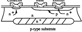
Figre 1.1 An integrated npn BJT.
Bipolar junction transistor (BJT) circuits 3 material interfacing on opposite sides to n-doped material. A pnp device can be created using an n-doped central region with p-doped interfacing regions. Since the npn type of BJT is more popular in present construction processes, the following discussion will center on this device.
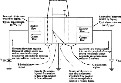
Figre 1.2 Distribution of electrons in the active region.
The geometry of the device implied in Fig. 1.2 is physically more like the earlier alloy transistor. This geometry is also capable of modeling the modern BJT (Fig. 1.1) as the theory applies almost equally well to both geometries. Normally, some sort of load would appear in either the collector or emitter circuit; however, this is not important to the initial discussion of BJT operation.
The circuit of Fig. 1.2 is in the active region, that is, the emitter-base junction is forward-biased, while the collector-base junction is reverse-biased. The current flow is controlled by the profile ...
Table of contents
- Cover Page
- Title Page
- Copyright Page
- Preface
- Editor-in-Chief
- Contributors
- 1: Bipolar Junction Transistor (BJT) Circuits
- 2: RF Passive IC Components
- 3: CMOS Amplifier Design
- 4: Bipolar Amplifier Design
- 5: High-Frequency Amplifiers
- 6: Operational Transconductance Amplifiers
- 7: Nyquist-Rate ADC and DAC
- 8: Oversampled Analog-to-Digital and Digital-to-Analog Converters
- 9: RF Communication Circuits
- 10: PLL Circuits
- 11: Continuous-Time Filters
- 12: Switched-Capacitor Filters
- 13: Materials
- 14: Compound Semiconductor Devices for Digital Circuits
- 15: Logic Design Principles and Examples
- 16: Logic Design Examples
Frequently asked questions
Yes, you can cancel anytime from the Subscription tab in your account settings on the Perlego website. Your subscription will stay active until the end of your current billing period. Learn how to cancel your subscription
No, books cannot be downloaded as external files, such as PDFs, for use outside of Perlego. However, you can download books within the Perlego app for offline reading on mobile or tablet. Learn how to download books offline
Perlego offers two plans: Essential and Complete
- Essential is ideal for learners and professionals who enjoy exploring a wide range of subjects. Access the Essential Library with 800,000+ trusted titles and best-sellers across business, personal growth, and the humanities. Includes unlimited reading time and Standard Read Aloud voice.
- Complete: Perfect for advanced learners and researchers needing full, unrestricted access. Unlock 1.5M+ books across hundreds of subjects, including academic and specialized titles. The Complete Plan also includes advanced features like Premium Read Aloud and Research Assistant.
We are an online textbook subscription service, where you can get access to an entire online library for less than the price of a single book per month. With over 1.5 million books across 990+ topics, we’ve got you covered! Learn about our mission
Look out for the read-aloud symbol on your next book to see if you can listen to it. The read-aloud tool reads text aloud for you, highlighting the text as it is being read. You can pause it, speed it up and slow it down. Learn more about Read Aloud
Yes! You can use the Perlego app on both iOS and Android devices to read anytime, anywhere — even offline. Perfect for commutes or when you’re on the go.
Please note we cannot support devices running on iOS 13 and Android 7 or earlier. Learn more about using the app
Please note we cannot support devices running on iOS 13 and Android 7 or earlier. Learn more about using the app
Yes, you can access Analog Circuits and Devices by Wai-Kai Chen in PDF and/or ePUB format, as well as other popular books in Technology & Engineering & Electrical Engineering & Telecommunications. We have over 1.5 million books available in our catalogue for you to explore.