![]()
Chapter 1
Introduction
1.1 The Nanotechnologies World
The term ‘nanotechnology’ indicates a multidisciplinary approach concerning materials, devices and systems in which at least one of the three characteristic dimensions of their components is measured at nanometric scale (nm), i.e., the billionth part of metre: 1 nm = 10–9 m.
The nanometric scale characterises:
(a) The atomic sizes, with atomic diameters going from 0.1 nm (He) to 0.67 nm (Cs) (computed using quantum mechanical calculations).
(b) The molecular dimensions (proteins have typical extension from 1–20 nm).
(c) The atoms’ distance at condensed matter level (the distance among sodium and chlorine ions in sodium chloride is 0.28 nm), is upto order of 100 nm for the smallest used components of microelectronics at the end of the twentieth century.
The submultiples of nanometre in the atomic world are more commonly expressed in angstrom (Å), with 1 Å = 0.1 nm = 10–10 m. The materials, whose structural and functional properties depend on components with at least one dimension at nanometric scale, are said nanostructural materials and the nanometric components are said nanostructures.
The nanotechnologies control and manipulate the matter at nanometric scale and try to use the properties and the chemical–physical phenomena appeared at such scale. Many empirical technologies of the past years have been totally or partially understood and reconsidered in relation to structures and mechanisms at nanolevel, as ceramics, metallurgy, photographic process, heterogeneous catalysis, resins and polymers and special compounds for pneumatic tyres.
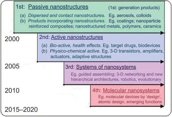
Nanophysics is commonly referred to as an intuition of Richard Feynman; in a famous conference of December 1959 by California Institute of Technology, he made forecasts around the possibility to control the matter and to realise devices at atomic scale, anticipating a great fields variety of scientific research and technical applications, that currently appear to be well developed. About that, we remember manufacture methods based on electronic and/or atomic beams, nanometric lithography, electronic microscopy, ‘single atom’ manipulation, electronics based on quantum and spin transport (so-called spintronics) and micro- and nano-opto-electro-mechanical systems, said respectively MOEMS and NOEMS. One of the first great step in such direction refers to the Japanese physicist Leo Esaki with the first realisation of a super network through a sequence of nanometric layers of different semiconductor materials (1969), opening the way to nanoelectronics. Eric Drexler of Massachusetts Institute of Technology (1977) put the experimental and computational basis of the conceptual and operational development for a lot of nanotechnologies. They assumed an important role in the succeeding ‘information era’, bringing to a scientific revolution comparable to the ‘microscale’ science and technology starting by 1970 (Fig. 1.1).
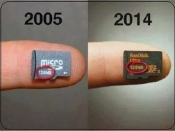
Electronics gave a strong impulse to the development of nanotechnologies through the progress in Physics, by which it depends on the fundamental understanding of processes at nanometric scale. The necessity to insert an always increasing number of electronic components in small volumes is due to both transportability and manageability demands of devices and also to the rapidity of calculation. Travelling electromagnetic signals at a finite speed (in 1 ns, the crossed distance is of the order of 30 cm), it is necessary that the central processing unit (CPU) of a calculator, able to perform 1 billion operations per second (1 Gflop), has smaller dimension than this length, so that only a negligible part of the calculation time is spent for the signal transmission to the components (Fig. 1.2).
Figure 1.1 Evolution of nanostructures and nanosystems.
Figure 1.2 Effect of miniaturisation: from 128 MB to 128 GB in the same space.
Being the number of placed electronic components of the order of millions, the respective dimensions have subsequently gone down (of the order of micrometre, μm). At such scale, electronics is commonly said microelectronics and it was developed through the invention of transistors (1947) and integrated circuits, in which the elementary components and the relative interconnections are realised on a single small plate (chip) of semiconductor material.
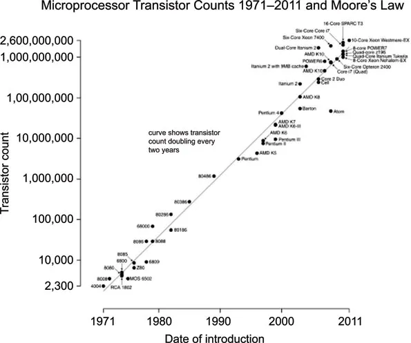
The number of active circuital elements in area unity is grown from 103 elements/cm2 (end of 1960) to 109 elements/cm2 and more, according to an exponential law known as Moore’s law (Fig. 1.3).
Figure 1.3 The Moore’s law.
The computer industry has kept on pushing the limits of miniaturisation and many current electronic devices have nanofeatures, whose origin is located in the computer industry, as compact disc (CD) and digital optical disc (DVD) players, cameras, inkjet printers, car airbag pressure sensors, etc.
Historically the Moore’s law has been followed and maintained by the microelectronics industry for three principal reasons:
(a) Economic reasons: The cost of a chip is essentially tied to the silicon occupied surface, so at parity of cost, the smallest transistors are more functional.
(b) Speed of work: Reducing the transistors dimension, the inner current increases and contemporarily the quantity of charge required for the gate for turning ON or OFF is reduced.
(c) Dissipated power: Reducing the device’s dimensions, reduces the number of necessary electrons for elaborating information, reducing consequently the dissipated energy for every calculation operation.
The integration level reached at the beginning of the twenty-first century entered in the nanometric domain, since the dimension of the smallest circuital elements used nowadays is broadly less than 100 nm. The distance going from the millimetric scale to 100 nm signs the integration levels, said respectively small-scale integrated (SSI), medium-scale integrated (MSI), large-scale integrated (LSI), very large-scale integrated (VLSI) and ultra large-scale integrated (ULSI). The integration of the components follows an ‘exponential-type’ growth too; it starts from multichip modules and becomes subsequently more rapid (by 2004) with the introduction of system-in-package (SIP) nanotechnologies and system-on-package (SOP) (Fig. 1.4).
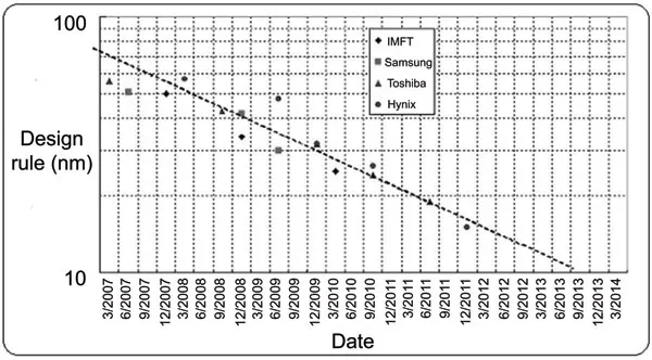
Figure 1.4 The trend of scaling for NAND flash memory allows doubling of components manufactured in the same wafer area in less than 18 months.
At the atomic scale, the physics of the electronic transport processes in semiconductors changes radically; the components and the interconnections become smaller with respect to two characteristic lengths:
(a) The electrons mean displacement: At such distances, it holds a motion without collisions from ordinarily ‘dissipative ohmic-type’, the transport regime becomes ballistic.
(b) The de Broglie wavelength of the electrons: It brings to the appearance of quantum effects as the discretisation of the energy levels.
In the zero-dimensional (0-D) nanostructures, such as atomic clusters, nanocrystals and quantum dots, the discrete energy levels move in an appreciable way through the addition or the subtraction of a single electric charge; it is possible to control the tunnel effect through the passage of a single electron (Coulomb blocking of tunnelling) controlling the transport of single carriers. This produces a conceptual revolution in the sector of electronics and a limit to the validity of Moore’s law in the present formulation. Another discriminating characteristic length among micro- and nanophysics is the wavelength of the electromagnetic waves at optical frequencies, corresponding to electronic energies of the order of 1 eV. It concerns the optoelectronic applications and the technical problems of microscopic observation, manufacture and checked manipulation of nanostructures. The observation and manipulation of matter at atomic scale have been possible through the invention of atomic force microscope (AFM), for its utility in the visualisation of non-conductive samples and for the manipulation at nanoscale, through a scanning tunnelling microscope (STM), coming to the great reached resolution of transmission electron microscope (TEM), laser scanning confocal microscopy (LSCM) and near-field scanning optical microscopy (NSOM). Such devices and techniques allow to visualise smaller objects than the wavelength of the utilised light. Many applications of nanotechnology range from simple to complex, as nanocoatings that can repel the dirt and reduce the need of dangerous cleaning agents, or mobile phones that are becoming smaller, cleverer and faster.
Nanotechnology, as ‘engineering at a very small scale’, can be applied to many areas of research and development, from medicine, manufacturing and computing to textiles and cosmetics, with a great impact on the everyday objects. It is providing solutions to many long-standing social, medical and environmental problems, in multidisciplinary research areas. For this reason, in particular at the phenomenological level, nanotechnology requires team efforts, including life scientists, biologists, biochemists, physicists, mathematicians, chemists, information technology experts and others.
In medicine, the improved knowledge of the body functioning at the cellular level is leading to new and better medical techniques, as the new ‘body friendly’ generation of implants, with a nanoscale topography that encourages acceptance by the cells in their surroundings (Fig. 1.5).
Figure 1.5 Schematic illustration showing how nanoparticles or other types of drugs can be used for the treatment of cancer.
The applications of nanotechnology for new materials are very important, for example, in the coatings sector; we know that polymer coatings are manifestly easily damaged and affected by heat. Adding only a small percentage (of the order of 2–3%) of nanoparticulate clay minerals to a polymer coating, they become more durable and scratch resistant. This implies the possibility to use these materials in particular situations of protection from an external potentially corrosive environment.
Particular nanocoatings can prevent the adherence of pictures and ‘graffiti’, allowing an easy removal with water once the coating has been applied, having therefore the important effect of improving the urban environment.
As nanoscale particles are below the wavelength of visible light, therefore, they can offer new properties with a big range of possible applications, such as fluorescent nanoparticles and quantum dots. They can be made to exhibit a range of colours, depending on their size and composition.
As for all scientific sectors, it is important to work seriously and carefully with nanomaterials; although they offer enormous opportunities, nanomaterials may also have risks to be taken into account for the realisation of the full benefits. There is the possibility that free nanoparticles of a specific length scale may be harmful to health, for example, if inhaled, particularly at the manufacturing stage. Industry and government must be conscious of this fact and must focus on identifying particles that may be hazardous to health or environment and studying how these risks may be quantified and minimised. In every case, nanotechnology has doubtless a large potential to bring benefits to society, but it must ensure these advances are as safe as possible.
1.2 Classification of Nanostructures
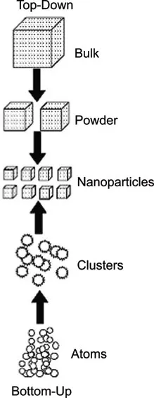
Two opposite procedures of manufacture of nanostructures are possible, i.e., ‘top-down’ and ‘bottom-up’. With the ‘top-down’ procedure, the obtained structures preserve the chemical–physical qualities of the started solids. In the ‘bottom-up’ procedure, it is possible to realise a great variety of nanostructured materials, also not existing in Nature, with non-ordinary properties and different from those of the usual crystalline materials of equal chemical composition (Fig. 1.6).
The small atomic or molecular clusters, composed of a number of atoms or molecules going from unities to a few thousands, form structures that can result very different by those of the respective solids and consequently their properties will be different; for example, small gold clusters have catalytic activity, while the crystalline material is notoriously inactive; the silicon clusters can be luminescent, while the crystalline silicon does not have this peculiarity. One of the key ideas of the ‘bottom-up’ procedure is the use of ‘pre-formed’ clusters as bricks for the construction of nanostructured materials, with the purpose to preserve on a macroscopic scale particular properties, typical of the clusters. Therefore, it becomes possible the realisation of materials with desired properties and high performance through the choice and control of their nanometric constituents. The combination of ‘top-down’ methods and tools with ‘self-assembly’ processes at atomic scale offers considerable and innovative opportunities to unite chemistry and biology parts to artificial structures created by man.
Figure 1.6 Schematic representation of the ‘top-down’ and ‘bottom-up’ procedures.
The manufacture procedures of nanostructured materials and systems depend on the nature of the ‘ground’ elements of nanometric dimension composing them; therefore, the nanostructures can be classified in relation to the respective elementary components. In particular:
(a) Atoms, inorganic molecules and metal-organic compounds: The first artificial nanostructures, realised in the last decades of 1900, were grown on a high regular surface of a solid substrate as a single ultra-thin films, quantum wells or multilayers formed by different materials, characterised by constant composition and thickness and totally controllable at atomic scale. The deposition techniques are based on the transport in the growth region of atoms or molecules:
(i) Either free (direct) adsorption in vapour state or transportation by chemical mixtures is don...