- 310 pages
- English
- ePUB (mobile friendly)
- Available on iOS & Android
eBook - ePub
About this book
Carbon nanotubes, with their extraordinary mechanical and unique electronic properties, have garnered much attention in the past five years. With a broad range of potential applications including nanoelectronics, composites, chemical sensors, biosensors, microscopy, nanoelectromechanical systems, and many more, the scientific community is more moti
Trusted by 375,005 students
Access to over 1.5 million titles for a fair monthly price.
Study more efficiently using our study tools.
Information
1: Structures and Properties of Carbon Nanotubes
Jie Han
NASA Ames Research Center
0–8493–2111–5/05/$0.00+$1.50
© 2005 by CRC Press LLC
Since the discovery of carbon nanotubes (CNTs) by Iijima in 1991 [1], great progress has been made toward many applications, including, for example:
- Materials
- Chemical and biological separation, purification, and catalysis
- Energy storage such as hydrogen storage, fuel cells, and the lithium battery
- Composites for coating, filling, and structural materials
- Devices
- Probes, sensors, and actuators for molecular imaging, sensing, and manipulation
- Transistors, memories, logic devices, and other nanoelectronic devices
- Field emission devices for x-ray instruments, flat panel display, and other vacuum nanoelectronic applications
The advantages of these applications have been demonstrated, including their small size, low power, low weight, and high performance, and will be discussed in the following chapters. These applications and advantages can be understood by the unique structure and properties of nanotubes, as outlined below:
- Structures (Sections 1.1–1.3)
- Bonding: sp2 hybrid orbital allows carbon atoms to form hexagons and occasionally pentagons and pentagon units by in-plane σ bonding and out-of-plane π bonding.
- Defect-free nanotubes: these are tubular structures of hexagonal network with a diameter assmall as 0.4 nm. Tube curvature results in σ-π rehybridization or mixing.
- Defective nanotubes: occasionally pentagons and heptagons are incorporated into a hexagonal network to form bent, branched, coroidal, helical, or capped nanotubes.
- Properties (Sections 1.4–1.9)
- Electrical: electron confinement along the tube circumference makes a defect-free nanotube either semiconducting or metallic with quantized conductance whereas pentagons and heptagons will generate localized states.
- Optical and optoelectronic: direct band gap and one-dimensional band structure make nano-tubes ideal for optical applications with wavelength ranging possibly from 300 to 3000 nm.
- Mechanical and electromechanical: σ-π rehybridization gives nanotubes the highest Young’s modulus of over 1 TPa and tensile strength of over 100 GPa and remarkable electronic response to strain and metal-insulator transition.
- Magnetic and electromagnetic: electron orbits circulating around a nanotube give rise to many interesting phenomena such as quantum oscillation and metalinsulator transition.
- Chemical and electrochemical: high specific surface and σ-π rehybridization facilitate molecular adsorption, doping, and charge transfer on nanotubes, which, in turn, modulates electronic properties.
- Thermal and thermoelectric: inherited from graphite, nanotubes display the highest thermal conductivity while the quantum effect shows up at low temperature.
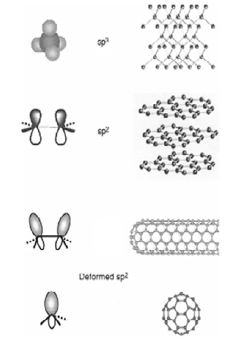
FIGURE 1.1 Bonding structures of diamond, graphite, nanotubes, and fullerenes: when a graphite sheet is rolled over to form a nanotube, the sp2 hybrid orbital is deformed for rehybridization of sp2 toward sp3 orbital or σ-π bond mixing. This rehybridization structural feature, together with π electron confinement, gives nanotubes unique, extraordinary electronic, mechanical, chemical, thermal, magnetic, and optical properties.
1.1 Bonding of Carbon Atoms
To understand the structure and properties of nanotubes, the bonding structure and properties of carbon atoms are discussed first. A carbon atom has six electrons with two of them filling the 1s orbital. The remaining four electrons fill the sp3 or sp2 as well as the sp hybrid orbital, responsible for bonding structures of diamond, graphite, nanotubes, or fullerenes, as shown in Figure 1.1.
In diamond [2], the four valence electrons of each carbon occupy the sp3 hybrid orbital and create four equivalent s covalent bonds to connect four other carbons in the four tetrahedral directions. This three-dimensional interlocking structure makes diamond the hardest known material. Because the electrons in diamond form covalent s bonds and no delocalized p bonds, diamond is electrically insulating. The electrons within diamond are tightly held within the bonds among the carbon atoms. These electrons absorb light in the ultraviolet region but not in the visible or infrared region, so pure diamond appears clear to human eyes. Diamond also has a high index of refraction, which makes large diamond single crystals gems. Diamond has unusually high thermal conductivity.
In graphite [3], three outer-shell electrons of each carbon atom occupy the planar sp2 hybrid orbital to form three in-plane s bonds with an out-of-plane p orbital (bond). This makes a planar hexagonal network. van der Waals force holds sheets of hexagonal networks parallel with each other with a spacing of 0.34 nm. The s bond is 0.14 nm long and 420 kcal/mol strong in sp2orbital and is 0.15 nm and 360 kcal/mol in sp3 configuration. Therefore, graphite is stronger in-plane than diamond. In addition, an outof- plane p orbital or electron is distributed over a graphite plane and makes it more thermally and electrically conductive. The interaction of the loose p electron with light causes graphite to appear black. The weak van der Waals interaction among graphite sheets makes graphite soft and hence ideal as a lubricant because the sheets are easy to glide relative to each other.
A CNT can be viewed as a hollow cylinder formed by rolling graphite sheets. Bonding in nanotubes is essentially sp2. However, the circular curvature will cause quantum confinement and s-p rehybridization in which three s bonds are slightly out of plane; for compensation, the p orbital is more delocalized outside the tube. This makes nanotubes mechanically stronger, electrically and thermally more conductive, and chemically and biologically more active than graphite. In addition, they allow topological defects such as pentagons and heptagons to be incorporated into the hexagonal network to form capped,bent, toroidal, and helical nanotubes whereas electrons will be localized in pentagons and heptagons because of redistribution of p electrons. For convention, we call a nanotube defect free if it is of only hexagonal network and defective if it also contains topological defects such as pentagon and heptagon or other chemical and structural defects.
Fullerenes (C60) are made of 20 hexagons and 12 pentagons [4]. The bonding is also sp2, although once again mixed with sp3 character because of high curvature. The special bonded structures in fullerene molecules have provided several surprises such as metalinsulator transition, unusual magnetic correlations, very rich electronic and optical band structures and properties, chemical functionalizations, and molecular packing. Because of these properties, fullerenes have been widely exploited for electronic, magnetic, optical, chemical, biological, and medical applications.
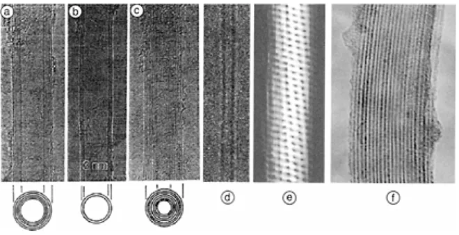
FIGURE 1.2 Homogeneous nanotubes of hexagonal network: TEM images (a),(b),and (c) for three multiwalled nanotubes (MWNTs) first discovered by Iijima in 1991 [1]; TEM image (d) for a single-wall nanotube (SWNT) first discovered by Iijima et al. in 1993 [5, 6], an atomic resolution STM image (e) for a SWNT; and a TEM image (f) for a SWNT rope first reported in 1996 by Thess et al. [7]. (Figures 1.2a and 1.2b are from Iijima, S., Nature, 354.56, 1991; Figure 1.2d is from Iijima, and Ichihashi, Nature, 363, 603, 1991; Figure 1.2f is from Thess et al, Science, 273, 483, 1996.)
1.2 Defect-Free Nanotube
There has been a tremendous amount of work studying defect-free nanotubes, including single or multiwalled nanotubes (SWNTs or MWNTs). A SWNT is a hollow cylinder of a graphite sheet whereas a MWNT is a group of coaxial SWNTs. SWNT was discovered in 1993 [5, 6], 2 years after the discovery of MWNT [1]. They are often seen as straight or elastic bending structures individually or in ropes [7] by transmission electron microscopy (TEM), scanning electron microscopy (SEM), atomic force microscopy (AFM), and scanning tunneling microscopy (STM). In addition, electron diffraction (EDR), x-ray diffraction (XRD), Raman, and other optical spectroscopy can be also used to study structural features of nanotubes. These characterization techniques will be discussed in detail in Chapter 5. Figure 1.2 shows an STM image with atomic resolution of a single SWNT from which one can see the hexagonal structural feature and TEM images of a SWNT rope and a few MWNTs.
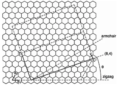
FIGURE 1.3 A nanotube (n,m) is formed by rolling a graphite sheet along the chiral vector C=na1+ma2 on the graphite where a1 and a2 are graphite lattice vector. The nanotube can also be characterized by the diameter |C| and the chiral angle θ is with respect to the zigzag axis, θ=0°. The diagram is constructed for a(8,4) nanotube.
A SWNT can be visualized as a hollow cylinder, formed by rolling over a graphite sheet. It can be uniquely characterized by a vector C in terms of a set of two integers (n,m) corresponding to graphite vectors a1 and a2 (F...
Table of contents
- Cover Page
- Title Page
- Copyright Page
- Preface
- The Editor
- Contributors
- 1: Structures and Properties of Carbon Nanotubes
- 2: Computational Nanotechnology of Carbon Nanotubes
- 3: Growth of Carbon Nanotubes by Arc Discharge and Laser Ablation
- 4: Growth: CVD and PECVD
- 5: Characterization Techniques in Carbon Nanotube Research
- 6: Applications in Scanning Probe Microscopy
- 7: Nanoelectronics Applications
- 8: Field Emission
- 9: Carbon Nanotube Applications: Chemical and Physical Sensors
- 10: Applications: Biosensors
- 11: Applications: Composites
- 12: Other Applications
Frequently asked questions
Yes, you can cancel anytime from the Subscription tab in your account settings on the Perlego website. Your subscription will stay active until the end of your current billing period. Learn how to cancel your subscription
No, books cannot be downloaded as external files, such as PDFs, for use outside of Perlego. However, you can download books within the Perlego app for offline reading on mobile or tablet. Learn how to download books offline
Perlego offers two plans: Essential and Complete
- Essential is ideal for learners and professionals who enjoy exploring a wide range of subjects. Access the Essential Library with 800,000+ trusted titles and best-sellers across business, personal growth, and the humanities. Includes unlimited reading time and Standard Read Aloud voice.
- Complete: Perfect for advanced learners and researchers needing full, unrestricted access. Unlock 1.5M+ books across hundreds of subjects, including academic and specialized titles. The Complete Plan also includes advanced features like Premium Read Aloud and Research Assistant.
We are an online textbook subscription service, where you can get access to an entire online library for less than the price of a single book per month. With over 1.5 million books across 990+ topics, we’ve got you covered! Learn about our mission
Look out for the read-aloud symbol on your next book to see if you can listen to it. The read-aloud tool reads text aloud for you, highlighting the text as it is being read. You can pause it, speed it up and slow it down. Learn more about Read Aloud
Yes! You can use the Perlego app on both iOS and Android devices to read anytime, anywhere — even offline. Perfect for commutes or when you’re on the go.
Please note we cannot support devices running on iOS 13 and Android 7 or earlier. Learn more about using the app
Please note we cannot support devices running on iOS 13 and Android 7 or earlier. Learn more about using the app
Yes, you can access Carbon Nanotubes by M. Meyyappan in PDF and/or ePUB format, as well as other popular books in Technology & Engineering & Industrial & Technical Chemistry. We have over 1.5 million books available in our catalogue for you to explore.