- 360 pages
- English
- ePUB (mobile friendly)
- Available on iOS & Android
eBook - ePub
DSP-Based Electromechanical Motion Control
About this book
Although the programming and use of a Digital Signal Processor (DSP) may not be the most complex process, utilizing DSPs in applications such as motor control can be extremely challenging for the first-time user. DSP-Based Electromechanical Motion Control provides a general application guide for students and engineers who want to implement DSP-base
Trusted by 375,005 students
Access to over 1.5 million titles for a fair monthly price.
Study more efficiently using our study tools.
Information
Chapter 1
INTRODUCTION TO THE TMSLF2407 DSP CONTROLLER
1.1 Introduction
The Texas Instruments TMS320LF2407 DSP Controller (referred to as the LF2407 in this text) is a programmable digital controller with a C2xx DSP central processing unit (CPU) as the core processor. The LF2407 contains the DSP core processor and useful peripherals integrated onto a single piece of silicon. The LF2407 combines the powerful CPU with on-chip memory and peripherals. With the DSP core and control-oriented peripherals integrated into a single chip, users can design very compact and cost-effective digital control systems.
The LF2407 DSP controller offers 40 million instructions per second (MIPS) performance. This high processing speed of the C2xx CPU allows users to compute parameters in real time rather than look up approximations from tables stored in memory. This fast performance is well suited for processing control parameters in applications such as notch filters or sensorless motor control algorithms where a large amount of calculations must be computed quickly.
While the “brain” of the LF2407 DSP is the C2xx core, the LF2407 contains several control-orientated peripherals onboard (see Fig. 1.1). The peripherals on the LF2407 make virtually any digital control requirement possible. Their applications range from analog to digital conversion to pulse width modulation (PWM) generation. Communication peripherals make possible the communication with external peripherals, personal computers, or other DSP processors. Below is a brief listing of the different peripherals onboard the LF2407 followed by a graphical layout depicted in Fig. 1.1.
The LF2407 peripheral set includes:
- Two Event Managers (A and B)
- General Purpose (GP) timers
- PWM generators for digital motor control
- Analog-to-digital converter
- Controller Area Network (CAN) interface
- Serial Peripheral Interface (SPI) – synchronous serial port
- Serial Communications Interface (SCI) – asynchronous serial port
- General-Purpose bi-directional digital I/O (GPIO) pins
- Watchdog Timer (“time-out” DSP reset device for system integrity)
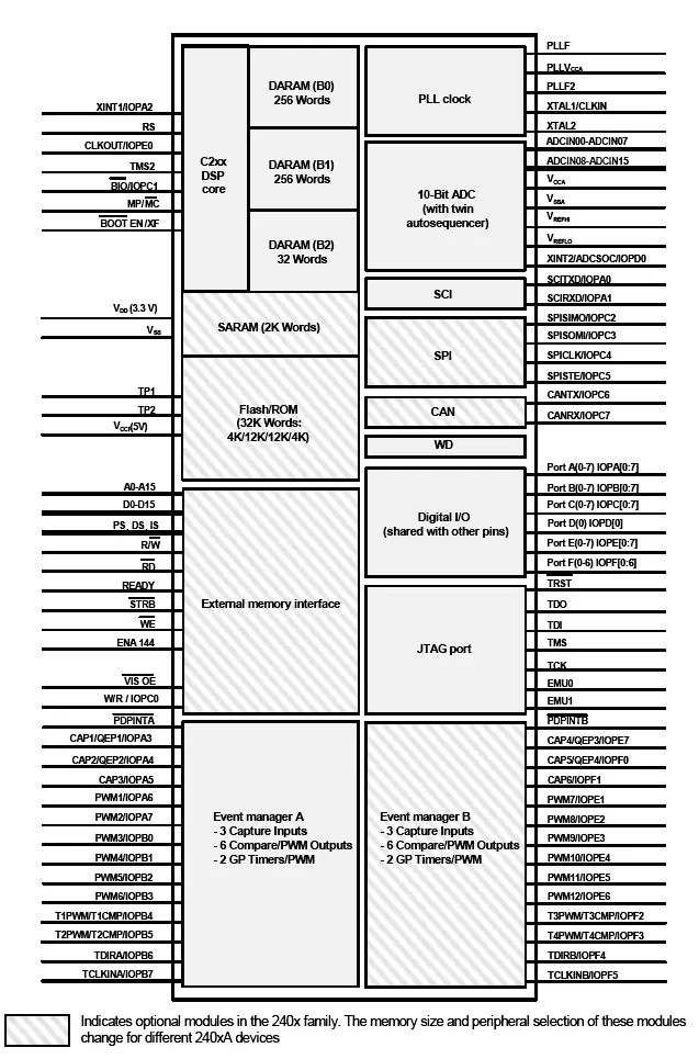
Figure 1.1 Graphical overview of DSP core and peripherals on the LF2407. (Courtesy of Texas Instruments)
1.2 Brief Introduction to Peripherals
The following peripherals are those that are integrated onto the LF2407 chip. Refer to Fig. 1.1 to view the pin-out associated with each peripheral.
Event Managers (EVA, EVB)
There are two Event Managers on the LF2407, the EVA and EVB. The Event Manager is the most important peripheral in digital motor control. It contains the necessary functions needed to control electromechanical devices. Each EV is composed of functional “blocks” including timers, comparators, capture units for triggering on an event, PWM logic circuits, quadrature-encoder–pulse (QEP) circuits, and interrupt logic.
The Analog-to-Digital Converter (ADC)
The ADC on the LF2407 is used whenever an external analog signal needs to be sampled and converted to a digital number. Examples of ADC applications range from sampling a control signal for use in a digital notch filtering algorithm or using the ADC in a control feedback loop to monitor motor performance. Additionally, the ADC is useful in motor control applications because it allows for current sensing using a shunt resistor instead of an expensive current sensor.
The Control Area Network (CAN) Module
While the CAN module will not be covered in this text, it is a useful peripheral for specific applications of the LF2407. The CAN module is used for multi-master serial communication between external hardware. The CAN bus has a high level of data integrity and is ideal for operation in noisy environments such as in an automobile, or industrial environments that require reliable communication and data integrity.
Serial Peripheral Interface (SPI) and Serial Communications Interface (SCI)
The SPI is a high-speed synchronous communication port that is mainly used for communicating between the DSP and external peripherals or another DSP device. Typical uses of the SPI include communication with external shift registers, display drivers, or ADCs.
The SCI is an asynchronous communication port that supports asynchronous serial (UART) digital communication between the CPU and other asynchronous peripherals that use the standard NRZ (non-return-to-zero) format. It is useful in communication between external devices and the DSP. Since these communication peripherals are not directly related to motion control applications, they will not be discussed further in this text.
Watchdog Timer (WD)
The Watchdog timer (WD) peripheral monitors software and hardware operations and asserts a system reset when its internal counter overflows. The WD timer (when enabled) will count for a specific amount of time. It is necessary for the user’s software to reset the WD timer periodically so that an unwanted reset does not occur. If for some reason there is a CPU disruption, the watchdog will generate a system reset. For example, if the software enters an endless loop or if the CPU becomes temporarily disrupted, the WD timer will overflow and a DSP reset will occur, which will cause the DSP program to branch to its initial starting point. Most error conditions that temporarily disrupt chip operation and inhibit proper CPU function can be cleared by the WD function. In this way, the WD increases the reliability of the CPU, thus ensuring system integrity.
General Purpose Bi-Directional Digital I/O (GPIO) Pins
Since there are only a finite number of pins available on the LF2407 device, many of the pins are multiplexed to either their primary function or the secondary GPIO function. In most cases, a pin’s second function will be as a general-purpose input/output pin. The GPIO capability of the LF2407 is very useful as a means of controlling the functionality of pins and also provides another method to input or output data to and from the device. Nine 16-bit control registers control all I/O and shared pins. There are two types of these registers:
- I/O MUX Control Registers (MCRx) – Used to control the multiplexer selection that chooses between the primary function of a pin or the generalpurpose I/O function.
- Data and Direction Control Registers (PxDATDIR) – Used to control the data and data direction of bi-directional I/O pins.
Joint Test Action Group (JTAG) Port
The JTAG port provides a standard method of interfacing a personal computer with the DSP controller for emulation and development. The XDS510PP or equivalent emulator pod provides the connection between the JTAG module on the LF2407 and the personal computer. The JTAG module allows the PC to take full control over the DSP processor while Code Composer StudioTM is running. Figure 1.2 shows the connection scheme from computer to the DSP board.
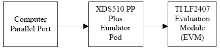
Figure 1.2 PC to DSP connection scheme.
Phase Locked Loop (PLL) Clock Module
The phase locked loop (PLL) module is basically an input clock multiplier that allows the user to control the input clocking frequency to the DSP core. External to the LF2407, a clock reference (can oscillator/crystal) is generated. This signal is fed into the LF2407 and is multiplied or divided by the PLL. This new (higher or lower frequency) clock signal is then used to clock the DSP core. The LF2407’s PLL allows the user to select a multiplication factor ranging from 0.5X to 4X that of the external clock signal. The default value of the PLL is 4X.
Memory Allocation Spaces
The LF2407 DSP Controller has three different allocations of memory it can use: Data, Program, and I/O memory space. Data space is used for program calculations, look-up tables, and any other memory used by an algorithm. Data memory can be in the form of the on-chip random access memory (RAM) or external RAM. Program memory is the location of user’s program code. Program memory on the LF2407 is either mapped to the off-chip RAM (MP/MC- pin =1) or to the on-chip flash memory (MP/MC- = 0), depending on the logic value of the MP/MC-pin.
I/O space is not really memory but a virtual memory address used to output data to peripherals external to the LF2407. For example, the digital-to-analog converter (DAC) on the Spectrum DigitalTM evaluation module is accessed with I/O memory. If one desires to output data to the DAC, the data is simply sent to the configured address of I/O space with the “OUT” command. This process is similar to writing to data memory except that the OUT command is used and the data is copied to and outputted on the DAC instead of being stored in memory.
1.3 Types of Physical Memory
Random Access Memory (RAM)
The LF2407 has 544 words of 16 bits each in the on-chip DARAM. These 544 words are partitioned into three blocks: B0, B1, and B2. Blocks B1 and B2 are allocated for use only as data memory. Memory block B0 is different than B1 and B2. This memory block is normally configured as Data Memory, and hence primarily used to hold data, but in the case of the B0 block, it can also be configured as Program Memory. B0 memory can be configured as program or data memory depending on the value of the core level “CNF” bit.
- (CNF=0) maps B0 to data memory.
- (CNF=1) maps B0 to program memory.
The LF2407 also has 2K of single-access RAM (SARAM). The addresses associated with the SARAM can be used for both data memory and program memory, and are software configurable to the internal SARAM or external memory.
Non-Volatile Flash Memory
The LF2407 contains 32K of on-chip flash memory that can be mapped to program space if the MP/MC-pin is made logic 0 (tied to ground). The flash memory provides a permanent location to store code that is unaffected by cutting power to the device. The flash memory can be electronically programmed and erased many times to allow for code development. Usually, the external RAM on the LF2407 Evaluation Module (EVM) board is used instead of the flash for code development due to the fact that a separate “flash programming” routine must be performed to flash code into the flash memory. The on-chip flash is normally used in situations where the DSP program needs to be tested where a JTAG connection is not practical or where the DSP needs to be tested as a “stand-alone” device. For example, if a LF2407 was used to develop a DSP control solution to an automobile braking system, it would be somewhat impractical to have a DSP/JTAG/PC interface in a car that is undergoing performance testing.
1.4 Software Tools
Texas Instrument’s Code Composer StudioTM (CCS) is a user-friendly Windows-based debugger for developing and debugging software for the LF2407. CCS allows users to write and debug code in C or in TI assembly language. CCS has many features that can aid in developing code. CCS features i...
Table of contents
- Cover Page
- Title Page
- Copyright Page
- Preface
- Acknowledgments
- Chapter 1
- Chapter 2
- Chapter 3
- Chapter 4
- Chapter 5
- Chapter 6
- Chapter 7
- Chapter 8
- Chapter 9
- Chapter 10
- Chapter 11
- Chapter 12
- Chapter 13
- Chapter 14
- Chapter 15
- Appendix A
Frequently asked questions
Yes, you can cancel anytime from the Subscription tab in your account settings on the Perlego website. Your subscription will stay active until the end of your current billing period. Learn how to cancel your subscription
No, books cannot be downloaded as external files, such as PDFs, for use outside of Perlego. However, you can download books within the Perlego app for offline reading on mobile or tablet. Learn how to download books offline
Perlego offers two plans: Essential and Complete
- Essential is ideal for learners and professionals who enjoy exploring a wide range of subjects. Access the Essential Library with 800,000+ trusted titles and best-sellers across business, personal growth, and the humanities. Includes unlimited reading time and Standard Read Aloud voice.
- Complete: Perfect for advanced learners and researchers needing full, unrestricted access. Unlock 1.5M+ books across hundreds of subjects, including academic and specialized titles. The Complete Plan also includes advanced features like Premium Read Aloud and Research Assistant.
We are an online textbook subscription service, where you can get access to an entire online library for less than the price of a single book per month. With over 1.5 million books across 990+ topics, we’ve got you covered! Learn about our mission
Look out for the read-aloud symbol on your next book to see if you can listen to it. The read-aloud tool reads text aloud for you, highlighting the text as it is being read. You can pause it, speed it up and slow it down. Learn more about Read Aloud
Yes! You can use the Perlego app on both iOS and Android devices to read anytime, anywhere — even offline. Perfect for commutes or when you’re on the go.
Please note we cannot support devices running on iOS 13 and Android 7 or earlier. Learn more about using the app
Please note we cannot support devices running on iOS 13 and Android 7 or earlier. Learn more about using the app
Yes, you can access DSP-Based Electromechanical Motion Control by Hamid A. Toliyat,Steven G. Campbell in PDF and/or ePUB format, as well as other popular books in Technology & Engineering & Electrical Engineering & Telecommunications. We have over 1.5 million books available in our catalogue for you to explore.