- 240 pages
- English
- ePUB (mobile friendly)
- Available on iOS & Android
eBook - ePub
Analog VLSI Design Automation
About this book
The explosive growth and development of the integrated circuit market over the last few years have been mostly limited to the digital VLSI domain. The difficulty of automating the design process in the analog domain, the fact that a general analog design methodology remained undefined, and the poor performance of earlier tools have left the analog
Trusted by 375,005 students
Access to over 1.5 million titles for a fair monthly price.
Study more efficiently using our study tools.
Information
Subtopic
Computer EngineeringChapter 1: Analog VLSI Design Automation
1.1 Introduction
With the rapid advance in IC manufacturing technology, the IC industry has shown a boom unprecedented in history. From a single transistor in the 1950s to ICs containing millions of transistors in the beginning of 21st century, the improvement in IC complexity and functionality has been exponential. This growing complexity has brought along design problems as well; an ever increasing number of designers are employed by IC providers. However, it has not been enough to simply hire more engineers, but it has been necessary to increase designer productivity. This has been possible only by the prevalent use of Computer- Aided Design (CAD) tools.
Many CAD tools for design automation exist in the literature. These tools are either university-based research tools or tools that can be acquired through well-established companies. Moreover, their common point is that they are all intended for use within a well-defined design flow. This design flow has shown few variations between companies over the last decade. Thus, phrases like Automatic Test Pattern Generation (ATPG), behavioral simulation, channel routing, synthesis, etc. have become well-defined terminology in digital IC design. When new tools are developed or existing tools are improved, they are expected to fit into this design flow, which is often summarized in terms of a Y-chart, as shown in Figure 1.1.
When we think about the analog design domain, we notice that such a design flow does not exist despite the recent efforts of some researchers. Thus, the research on analog design automation, which has been very limited as opposed to digital design automation, has concentrated mostly either on specific tools designed for specific applications, or on tools targeted toward specific aspects of a design. The best-known example of the latter case is SPICE and its many variants. SPICE is an excellent tool for circuit-level simulation, but where it fits in a design flow is an open question. Many examples from the literature will be cited for the former case in later chapters of this book.
The major reason underlying this lack in analog design automation tools has been the difficulty of the problem, in our opinion. Design in the analog domain requires creativity because of the large number of free parameters and the sometimes obscure interactions between them. Traditionally, analog designs have been carried out by experienced designers whose only aid is SPICE for simulation. These designers have not been able to quantify their knowledge in a formal framework suitable for CAD tools. Thus, analog design has remained more of an “art” than a “science”.
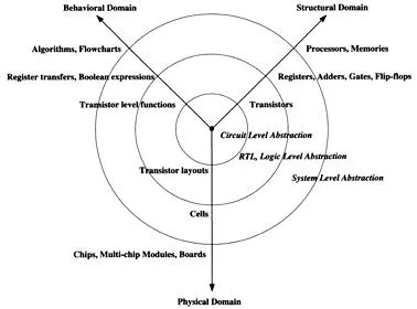
FIGURE 1.1 Y-chart showing design domains and abstraction levels.
The situation described above cannot continue in this direction in the future for several reasons. A short time-to-market is a big pressure on all designers. Using modern computers and Design Automation (DA) software, digital designers are able to design multi-million transistor chips in less than a year, whereas a team of analog designers may require a similar time to design an analog chip (or an analog section of a chip) consisting of a few hundred transistors. Furthermore, when the technology changes, the digital designers can update or adapt their designs in a matter of weeks, whereas the analog designers may require a time similar to the original design time.
In recent years, the IC Design industry has been moving to System-On-Chip (SOC) designs, where a single chip may contain both analog and digital circuits. For example, an SOC aimed at processing information acquired through radio transmission and acting on it may require an RF receiver, A/D converter, a microprocessor, a RAM block, a ROM block, digital circuitry for connecting to the ethernet, a D/A converter, filters and even some type of actuators. Typically, a designer, or even a company, cannot be an expert on all these different fields and may choose to use the designs of others. This brings us to the concept of intellectual property (IP) reuse in IC Design. IP reuse and the associated procedures have been around for the last 10 years and are slowly becoming an established discipline for digital design where the IP consists of a behavioral definition that can be synthesized targeting the end-user’s technology. However, the same idea cannot be applied for analog design, where changes in technology may even dictate different circuits for the same application. To apply IP reuse in the analog domain, an Analog Design Automation (ADA) environment must be defined.
In this book, we propose a general methodology that can be used for many different applications. The design flow is created such that each tool is well-defined in terms of its duties, its inputs, and its outputs. The tools presented in subsequent chapters are state-of-the-art tools developed over the years by our research group, but new tools conforming to the definition of the design flow can be developed and these tools can replace our own. Furthermore, the design flow has been defined such that each tool is also useful by itself and the designer may choose to use them independently. The designer may also intervene at any point, choosing to bypass some of the tools and use his/her own intuition. As the reader proceeds through the book, he/she should keep this philosophy in mind.
We also illustrate our approach on three examples in this book. These examples are taken from the verbal definition phase to the physical layout generation phase. Their results are compared with the initial verbal specifications. The design examples chosen are Switched Capacitor (SC) filters, A/D converters, and Analog Neural Networks. SC filters are chosen to illustrate the performance of our system on sampled-data systems. A/D converters are the most common example of mixed-signal systems. Analog Neural Networks provide an example of continuous-time analog arithmetic systems.
In the next section of this chapter, a brief literature survey on complete analog CAD frameworks and terminology will be presented. Section 1.3 will describe our design flow and the associated design tools in our design flow. Section 1.4 concluding this chapter will outline the three examples that will be pursued throughout the book. Also, a very brief outline of the remaining chapters of this book can be found in this section.
1.2 Previous Analog Design Flows
A complete and rather recent overview on analog CAD can be found in Reference [1]. The authors review over a hundred different works on analog CAD ranging from macromodeling at the behavioral level to layout at the lowest level. They also outline a hierarchical design methodology similar to ours in many respects. Their methodology consists of a top-down synthesis and a bottom-up verification at every level of the hierarchy. Starting from a system concept, they first carry out their system design followed by simulation and verification. The system design is then given as input to the architectural design phase, which is the input to the cell design, cell layout, and system layout phases. Each of these phases has a feedback loop consisting of simulation and verification as shown in Figure 1.2. The top-down direction is called forward progress, whereas the bottom-up phase is called backtracking and redesign.

FIGURE 1.2 Analog IC design process.
Each block in the top-down direction takes an architecture or topology from the preceding block as well as performance constraints. Its output is a more detailed circuit diagram (or finally layout) as well as new specifications for the next block. Thus, each block in the forward direction does a specification translation and topology selection (Figure 1.3).
The advantage of propagating the constraints down the design hierarchy is that problems or inconsistencies in the specifications can be caught early on. Therefore, the ADA design flow requires tools for simulation at several levels of the design hierarchy, modeling at high levels, circuit synthesis, and layout generation. We will briefly review each of these in the next few paragraphs, leaving detailed description of existing tools to subsequent chapters.
One of the major tasks in ADA is simulation. Traditionally, this task has come to denote simulation at the circuit level and this is done numerically through SPICE. However, circuit simulation is not adequate or suited for many applications in ADA. For example, using traditional SPICE in a mixed signal circuit takes a huge amount of time where the digital sections could easily be simulated by a logic simulator. Also, simulating discrete time systems like SC filters or Σ-Δ modulators is time consuming, to say the least. For such systems, special numerical simulators must be developed. Another simulation application where SPICE is not suitable is in cases where the user would like to estimate the performance of a large circuit consisting of well-defined blocks to a certain accuracy. In such a case, using analytical models for the blocks forming the large circuit not only speeds up the simulation, but also gives the designer insight on how the overall circuit performance depends on a particular property of a certain block. Such models can be written in analog HDL’s like AHDL or VHDL-AMS developed specifically for such applications. Another possibility for modeling blocks within a complex system is the use of macromodels, which are highly simplified circuits approximating the behavior of the block. For example, an opamp can be represented by a voltage controlled voltage source and a resistor. The advantage of using a macromodel is that a special simulator is not required, but SPICE will still do the simulation. One final application in ADA where simulation is required is in estimating the performance of a circuit before designing it. This is a very important problem for ADA that has not been satisfactorily solved and will be discussed in detail in the second chapter of this book.

FIGURE 1.3 Hierarchical design strategy.
Another type of simulation at the circuit level is symbolic analysis. Symbolic analysis is fundamentally different from numerical simulation, which tries to solve the circuit via nodal analysis by substituting element models into the nodal voltage matrix. The intermediate steps in a numerical simulator are meaningless to the human. On the contrary, symbolic analysis tries to derive equations for the circuit. For example, symbolic analysis will derive equations pertaining to the gain of an opamp based on the transconductance (gm) and output impedance (go) of the transistors composing it. At first glance, this type of analysis seems very advantageous, as it makes the simulation very fast once the equations have been derived. Even more important, it gives the designer insight on how to design the circuit and which parameters are critical. However, symbolic analysis has several shortcomings. One of these is that DC analysis has to be performed for the transistor small signal parameters to be obtained. Thus, SPICE is still necessary for the solution. The second shortcoming is that the computer may generate huge expressions for medium complexity circuits that are not easy to simulate and much harder to interpret. Recently, several symbolic analyzers have been introduced, which can do simplification on these equations, even while generating them. However, symbolic analysis is not an alternative to SPICE analysis, but it complements it in some respects. It is an alternative to deriving equations by hand.
Another tool that is necessary for ADA is analog circuit synthesis and optimization. Analog circuit synthesis is the opposite of circuit simulation. That is, an analog circuit synthesis tool tries to generate a circuit that meets some given specifications. In doing this, the tool performs mainly two tasks; topology selection and circuit sizing. Given a certain set of specifications, one must try to find the optimum topology within certain constraints while minimizing some cost. This is called topology selection and is the more difficult of these two problems. Some kind of library is necessary for topology selection. However, even with a library, it is not obvious as to which topology is going to yield the best results. For example, to attain a certain voltage gain, a two stage opamp may be enough. However, the transistor sizes of the two stage opamp may have to be so large to reach that gain that a three stage opamp with smaller transistors might yield a smaller area. Thus, selecting the suitable topology without transistor size information is very difficult. Most topology selection algorithms to date have been rather heuristic in nature and try to use the expert knowledge of the designer.
The second problem in analog circuit synthesis is circuit sizing. Here, the sizing and biases of all devices in a selected topology have to be determined according to the given specifications. This can be done either in a knowledge-based manner or by pure optimization. The older synthesizers were mostly knowledgebased, where the knowledge of how to optimize the topology was somehow encoded into the software. However, with the improvement in the performance of computers, optimization-based synthesizers started coming into play in the late 1980s. Optimization can be done either on equations or on simulations. In either case, the optimization problem is not a simple one and contains many local minima, thus requiring the utilization of special optimizers. Analog circuit sizing is one of the best-studied subjects in ADA and there is a plethora of literature on analog circuit sizing, which will be reviewed and classified in Chapter 3 of this book.
Layout synthesis is yet another tool that is requ...
Table of contents
- Cover Page
- Half Title
- Series Page
- Title Page
- Copyright Page
- Dedication
- Preface
- Acknowledgments
- About the Authors
- List of Figures
- List of Tables
- Table of Contents
- 1 Analog VLSI Design Automation
- 2 System-Level Design Automation
- 3 Circuit Level Synthesis
- 4 Layout-Level Design Automation
- 5 Design Automation Case Studies
- 6 Conclusion and Future Directions
- Appendix A CMOS Spice Models Index
Frequently asked questions
Yes, you can cancel anytime from the Subscription tab in your account settings on the Perlego website. Your subscription will stay active until the end of your current billing period. Learn how to cancel your subscription
No, books cannot be downloaded as external files, such as PDFs, for use outside of Perlego. However, you can download books within the Perlego app for offline reading on mobile or tablet. Learn how to download books offline
Perlego offers two plans: Essential and Complete
- Essential is ideal for learners and professionals who enjoy exploring a wide range of subjects. Access the Essential Library with 800,000+ trusted titles and best-sellers across business, personal growth, and the humanities. Includes unlimited reading time and Standard Read Aloud voice.
- Complete: Perfect for advanced learners and researchers needing full, unrestricted access. Unlock 1.5M+ books across hundreds of subjects, including academic and specialized titles. The Complete Plan also includes advanced features like Premium Read Aloud and Research Assistant.
We are an online textbook subscription service, where you can get access to an entire online library for less than the price of a single book per month. With over 1.5 million books across 990+ topics, we’ve got you covered! Learn about our mission
Look out for the read-aloud symbol on your next book to see if you can listen to it. The read-aloud tool reads text aloud for you, highlighting the text as it is being read. You can pause it, speed it up and slow it down. Learn more about Read Aloud
Yes! You can use the Perlego app on both iOS and Android devices to read anytime, anywhere — even offline. Perfect for commutes or when you’re on the go.
Please note we cannot support devices running on iOS 13 and Android 7 or earlier. Learn more about using the app
Please note we cannot support devices running on iOS 13 and Android 7 or earlier. Learn more about using the app
Yes, you can access Analog VLSI Design Automation by Sina Balkir,Günhan Dündar,A. Selçuk Ögrenci in PDF and/or ePUB format, as well as other popular books in Technology & Engineering & Computer Engineering. We have over 1.5 million books available in our catalogue for you to explore.