eBook - ePub
Metal Oxide Nanostructures
Synthesis, Properties and Applications
- 328 pages
- English
- ePUB (mobile friendly)
- Available on iOS & Android
eBook - ePub
Metal Oxide Nanostructures
Synthesis, Properties and Applications
About this book
Metal Oxide Nanostructures: Synthesis, Properties and Applications covers the theoretical and experimental aspects related to design, synthesis, fabrication, processing, structural, morphological, optical and electronic properties on the topic. In addition, it reviews surface functionalization and hybrid materials, focusing on the advantages of these oxide nanostructures. The book concludes with the current and future prospective applications of these materials. Users will find a complete overview of all the important topics related to oxide nanostructures, from the physics of the materials, to its application.
- Delves into hybrid structured metal oxides and their promising use in the next generation of electronic devices
- Includes fundamental chapters on synthesis design and the properties of metal oxide nanostructures
- Provides an in-depth overview of novel applications, including chromogenics, electronics and energy
Trusted by 375,005 students
Access to over 1.5 million titles for a fair monthly price.
Study more efficiently using our study tools.
Information
1
Introduction
Abstract
Nanotechnology is a multidisciplinary field of research with emerging applications in several areas, such as materials, physics, chemistry, engineering, and medicine.
This chapter gives a general overview of the importance of nanotechnology, and of metal oxide nanostructures in particular, as well as its impact on society.
Keywords
Billionth; medicine; environment; metal oxide nanostructures; energy; information; nanotoxicology
1.1 Nanoscience and nanotechnology
The prefix nano is a Greek numerical word that refers to a billionth, where a nanometer is one billionth of a meter (10−9 m). As an outcome, nanoscience studies the phenomena, properties, and responses of materials at atomic, molecular, and macromolecular scales, while nanotechnology is the design, manipulation, building, production, and application of structures, devices, and systems with sizes below 100 nm. In this scale, and especially below 5 nm, the optical, electrical, and structural properties of matter differ significantly from that in bulk [1].
Taking these phenomena into consideration, nanotechnology is considered as an emerging technology due to the possibility to improve well-established products and to create new products and devices with totally new characteristics and functions with enormous potential in a wide range of applications. Significant applications of nanoscience and nanoengineering are already perceived in the fields of pharmaceutics, cosmetics, processed food, chemical engineering, high-performance materials, electronics, precision mechanics, optics, energy production, and environmental sciences. Furthermore, great nanotechnological innovations are anticipated to happen in information and communication, biology, medicine, and metrology.
Formerly in the European action plan of nanosciences and nanotechnologies for 2005–09 it was mentioned that “Nanotechnology is an area which has highly promising prospects for turning fundamental research into successful innovations. Not only to boost the competitiveness of our industry but also to create new products that will make positive changes in the lives of our citizens, be it in medicine, environment, electronics or any other field. Nanosciences and nanotechnologies open up new avenues of research and lead to new, useful, and sometimes unexpected applications. Novel materials and new-engineered surfaces allow making products that perform better. New medical treatments are emerging for fatal diseases, such as brain tumors and Alzheimer’s disease. Computers are built with nanoscale components and improving their performance depends upon shrinking these dimensions yet further” [2].
Nanotechnology is an emerging and dynamic field with many potential application areas, coupled with great potential benefits, but also risks, for society. Products containing nanostructured materials are already in the market. The range of commercial products available today is very broad, including metals, ceramics, polymers, smart textiles, cosmetics, sunscreens, electronics, paints, and varnishes. However, new methodologies and instrumentation have to be developed in order to increase our knowledge and information on their properties. Nanomaterials must be examined for potential effects on health as a matter of precaution, and their possible environmental impacts. The development of specific guidance documents at a global level for the safety evaluation of nanotechnological products is still lacking. Ethical and moral concerns also need to be addressed in parallel with the new developments. While products based on nanotechnology are actually reaching the market, sufficient knowledge on the associated toxicological risks is still lacking. Reducing the size of structures to the nano level originates rather distinct properties. Together with the chemical composition, which largely dictates the intrinsic toxic properties, very small size appears to be a dominant indicator for drastic or toxic effects of particles. From a regulatory point of view, a risk management strategy is already a requirement for all medical technology applications.
Huge aspirations are coupled to nanotechnological developments in modern medicine. The potential medical applications are predominantly in diagnostics (disease diagnosis and imaging), monitoring, the availability of more durable and better prosthetics, and new drug-delivery systems for potentially harmful drugs [3].
Nanoscience and nanotechnology is one of the most visible and growing research areas in science and technology, and all over the world research funding agencies have been supporting the exploitation of the potentialities of this field in the areas of chemistry, materials, engineering, and medicine. Nanoscience and nanotechnology are fueling a new industrial revolution supported by the scientific ability to fabricate, model, and manipulate objects with a small numbers of atoms, and the almost daily discovery of new phenomena at the nanoscale [4,5].
1.2 History of nanotechnology
The term “nanotechnology” was introduced by Norio Taniguchi in 1974 during a scientific conference [6], but the idea of building “small” things is usually attributed to Richard Feynman based on the talk he gave in 1959. He predicted that machines would build smaller machines and other products with atom by atom control, a process which was later called molecular manufacturing [7].
Truthfully, the study of interfaces and colloids started nearly a century before they became associated with nanotechnology. The first observations and size measurements of nanoparticles were performed at the start of the 20th century by Richard Zsigmondy, winner of the 1925 Nobel Prize in Chemistry for his demonstration of the heterogeneous nature of colloid solutions and for the methods he used, which have since become fundamental in modern colloid chemistry [8,9]. Zsigmondy was the first to use the term “nanometer” explicitly for characterizing particle sizes. At the same time, Irving Langmuir, winner of the 1932 Nobel Prize in Chemistry, introduced the concept of a monolayer, a layer of material one molecule thick [10].
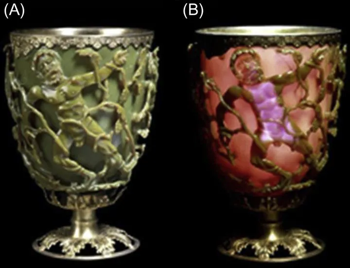
The use of nanostructured materials is not a recently discovered era. It dates back to the fourth century AD when Romans were using nano-sized metals to decorate glasses and cups. One of the first known, and most famous example, is the Lycurgus cup (Fig. 1.1), which was fabricated from nanoparticles of gold and silver that were embedded in the glass [3].
Later, the major boost to further develop nanotechnology was achieved in 1981 by Gerd Binnig and Heinrich Rohrer at IBM (International Business Machines), Zurich Research Laboratory with the invention of the scanning tunneling microscope (STM), for which they were awarded the Nobel Prize in Physics in 1986 [12]. In 1985 Binnig, Calvin Quate, and Christoph Gerber invented the atomic force microscope (AFM) [13]. Still in this year, the first fullerene was discovered by Harry Kroto, Richard Smalley, and Robert Curl, who together won the 1996 Nobel Prize in Chemistry [14]. The discovery of carbon nanotubes, even if generally attributed to Sumio Iijima due to the impact of his “Nature” paper in 1991 [15], was first published in 1952 by L. V. Radushkevich and V. Lukyanovich, but in Russian [16]. In the year after, Eric Dexter published the book “Engines of Creation” and he is described as the founding father of nanotechnology. He established the main fundamentals of molecular engineering and described the implementation and applications of advanced nanotechnologies [17]. Drexler was also one of the cofounders of the Foresight Institute that is: “the primary force pushing for the kind of nanotechnology that will truly transform our future, from medicine to the environment to space settlement” [18].
In 1999, Chad Mirkin at Northwestern University invented dip-pen nanolitography (DPN), leading to the manufacture of reproducible “writing” of electronic circuits as well as patterning of biomaterials for cell biology research, nanoencryption, and other applications. In the beginning of 2000 the first consumer products making use of nanotechnology began to appear in the marketplace, including lightweight nanotechnology, enabled automobile bumpers that resist denting and scratching, golf balls that fly straighter, tennis rackets that are stiffer (therefore, the ball rebounds faster), baseball bats with better flex and “kick,” nano-silver antibacterial socks, clear sunscreens, wrinkle- and stain-resistant clothing, deep-penetrating therapeutic cosmetics, scratch-resistant glass coatings, faster-recharging batteries for cordless electric tools, and improved displays for televisions, cell phones, and digital cameras.
In Europe, the research and interest in nanotechnology also started to grow. In 2004 the European Commission promoted the communication “Towards a European Strategy for Nanotechnology” [19] and in 2008 released the “Code of conduct for responsible nanosciences and nanotechnologies research” [20].
In 2013, IBM launched “A Boy and His Atom: The World’s Smallest Movie” in which the atoms are moved by using their STM and recorded in a movie to further promote IBM’s research in the field of atomic-scale memory and to reveal the latest developments and new possibilities in nanotechnology (Fig. 1.2) [21].

1.3 Nanotechnology in the real world
The first type of nanostructure employed in consumer products was in nanopowder form without any manipulatio...
Table of contents
- Cover image
- Title page
- Table of Contents
- Copyright
- Dedication
- About the series editor
- About the authors
- Foreword
- Preface to the series
- Preface
- Acknowledgments
- 1. Introduction
- 2. Synthesis, design, and morphology of metal oxide nanostructures
- 3. Structural, optical, and electronic properties of metal oxide nanostructures
- 4. Chromogenic applications
- 5. Electronic applications of oxide nanostructures
- 6. Oxide materials for energy applications
- 7. Oxide nanoparticle hybrid materials and applications
- 8. Conclusions and future perspectives
- Index
Frequently asked questions
Yes, you can cancel anytime from the Subscription tab in your account settings on the Perlego website. Your subscription will stay active until the end of your current billing period. Learn how to cancel your subscription
No, books cannot be downloaded as external files, such as PDFs, for use outside of Perlego. However, you can download books within the Perlego app for offline reading on mobile or tablet. Learn how to download books offline
Perlego offers two plans: Essential and Complete
- Essential is ideal for learners and professionals who enjoy exploring a wide range of subjects. Access the Essential Library with 800,000+ trusted titles and best-sellers across business, personal growth, and the humanities. Includes unlimited reading time and Standard Read Aloud voice.
- Complete: Perfect for advanced learners and researchers needing full, unrestricted access. Unlock 1.5M+ books across hundreds of subjects, including academic and specialized titles. The Complete Plan also includes advanced features like Premium Read Aloud and Research Assistant.
We are an online textbook subscription service, where you can get access to an entire online library for less than the price of a single book per month. With over 1.5 million books across 990+ topics, we’ve got you covered! Learn about our mission
Look out for the read-aloud symbol on your next book to see if you can listen to it. The read-aloud tool reads text aloud for you, highlighting the text as it is being read. You can pause it, speed it up and slow it down. Learn more about Read Aloud
Yes! You can use the Perlego app on both iOS and Android devices to read anytime, anywhere — even offline. Perfect for commutes or when you’re on the go.
Please note we cannot support devices running on iOS 13 and Android 7 or earlier. Learn more about using the app
Please note we cannot support devices running on iOS 13 and Android 7 or earlier. Learn more about using the app
Yes, you can access Metal Oxide Nanostructures by Daniela Nunes,Ana Pimentel,Lidia Santos,Pedro Barquinha,Luis Pereira,Elvira Fortunato,Rodrigo Martins,Luís Miguel Nunes Pereira, Ghenadii Korotcenkov in PDF and/or ePUB format, as well as other popular books in Technology & Engineering & Materials Science. We have over 1.5 million books available in our catalogue for you to explore.