- 470 pages
- English
- ePUB (mobile friendly)
- Available on iOS & Android
eBook - ePub
Handbook of Thin Film Deposition
About this book
Handbook of Thin Film Deposition, Fourth Edition, is a comprehensive reference focusing on thin film technologies and applications used in the semiconductor industry and the closely related areas of thin film deposition, thin film micro properties, photovoltaic solar energy applications, materials for memory applications and methods for thin film optical processes. The book is broken up into three sections: scaling, equipment and processing, and applications. In this newly revised edition, the handbook will also explore the limits of thin film applications, most notably as they relate to applications in manufacturing, materials, design and reliability.
- Offers a practical survey of thin film technologies aimed at engineers and managers involved in all stages of the process: design, fabrication, quality assurance, applications and the limitations faced by those processes
- Covers core processes and applications in the semiconductor industry and new developments within the photovoltaic and optical thin film industries
- Features a new chapter discussing Gates Dielectrics
Trusted by 375,005 students
Access to over 1.5 million titles for a fair monthly price.
Study more efficiently using our study tools.
Information
Section II
Thin Film Deposition Equipment & Processing
Outline
Chapter 5
Limits of Gate Dielectrics Scaling
Shahab Siddiqui1, Takashi Ando2, Rajan K. Pandey1 and Dominic Schepis1, 1Globalfoundries, Malta, NY, United States, 2IBM T. J. Watson Research Center, Yorktown, NY, United States
Abstract
This chapter discusses limits of gate dielectric scaling for advanced metal oxide semiconductor field effect transistor (MOSFET). We will review details of hafnium oxide (HfO2) gate oxide and how HfO2 can be modified to hafnium oxynitrides (HfON) and hafnium lanthanum oxynitrides (HfLaON) to increase dielectric constant for continuous equivalent oxide thickness (EOT) scaling. Bilayer hafnium oxide/titanium oxide (HfO2/TiO2) as a higher ‘k’ dielectric option for FinFET gate length (Lg) scaling is discussed. Interfacial layer (IL) scaling technologies for overall EOT scaling are also covered in this chapter. Ab-initio modeling results to evaluate ternary and quaternary gate oxide for higher ‘k’ dielectrics options, and effective metal work functions calculations to optimize and develop new metal gates are discussed. New gate dielectric reliability failure mechanisms due to three dimensional natures of FinFET devices are reviewed.
Thermal oxide equivalent quality deposited silicon dioxide (SiO2) using atomic layer deposition (ALD) with post-treatments (e.g., plasma nitridation and anneals) as a high voltage input/output (I/O) gate oxide with silicon-germanium channel (SiGe) results are shown. Finally, we give a brief overview of silicon germanium pFET channel material as a gate dielectric scaling knob, and how it can enable continued EOT scaling without reliability degradation.
Keywords
Gate dielectrics scaling; hafnium oxynitrides; hafnium lanthanum oxynitrides; bilayer oxide; interfacial layer; deposited SiO2; FinFETs; silicon-germanium channel
5.1 Introduction
Silicon dioxide as a gate oxide reached its scaling limit somewhere around 90-nm to 65-nm technology node due to excessive leakage below 1 nm physical oxide thickness. To overcome silicon dioxide scaling limits, hafnium oxide as a high-k dielectric material was introduced in the 45-nm node. Introduction of high k dielectric as a gate oxide enabled gate length and equivalent oxide thickness (EOT) scaling for improved device performance and area scaling. However, further physical scaling of hafnium dioxide (HfO2) looks difficult due to increased leakage below 1.5 nm physical thickness. For continued scaling other device innovations such as Fin Shaped Field Effect Transistor (FinFET) and fully depleted SOI (FDSOI) technologies have been introduced. Introduction of FinFET allowed us to relax EOT criteria due to excellent short channel control of FinFET devices, however, future gate length scaling of FinFET devices still require EOT to be scaled, especially for ultra-low threshold devices. In this chapter, we will discuss current status of hafnium oxide as a replacement for SiO2, and how EOT can be scaled practically by modifying HfO2, for example by doping hafnium oxide to form HfOxN, HfLaOxN, and potentially some bilayer dielectrics such as HfO2/TiO2 to increase k-value of the dielectric stack without changing the entire material system in gate stack. These modified HfO2 systems are practical approaches and have the potential to be implemented at future highly scaled FinFET, FDSOI devices and beyond FinFETs such as gate all around (GAA), and alternative channel (SiGe and Ge) based FinFET and nanowire devices.
We will discuss innovation in high-voltage input/output (I/O) devices gate oxide due to dual channel planar high-performance devices, and later in highly scaled FinFET to gate all-around architecture. The rise of system on chip (SoC) and Hik/Metal gate requires careful integration of thin film gate oxide processes for I/O oxide. It is evident that I/O oxide will play a critical role in FinFET and GAA schemes for overall transistor strategy as we push forward on transistor scaling beyond 5 nm FinFET and new device architectures such as GAA and alternate channel substrates.
Silicon germanium channels as mobility enhancements, and gate oxide scaling knob results will be reviewed. In this chapter, we will also review how ab initio calculations (density functional theory) are playing a role in developing gate oxides and overall stack by providing guidance to technologists and engineers, and how gate dielectrics can be optimized by utilizing ab initio calculations as tools available to technologists, material chemists, and the semiconductor process research and development community.
Finally we will summarize potential device architecture options beyond FinFET and how gate oxide integration will play a critical role in enablement of nano electronics devices, and pushing the physical scaling and capabilities.
5.2 Dennard Scaling Theory
In early 1970s Robert Dennard at IBM Research introduced the principle of MOS transistor scaling called “Dennard’s scaling theory” [1]. It would not be an overreach to claim that Dennard scaling theory is the foundation which drove significant innovation in complementary metal-oxide-semiconductor (CMOS) miniaturization for over 30 years, covering device design, device integration, lithography processes, equipment innovation, silicon processes and materials breakthroughs. Dennard scaling theory will be discussed in detail in the next section.
5.2.1 Constant Electric-Field Scaling
The basic idea of scaling, shown in Fig. 5.1, is to reduce the dimensions of the MOS transistors and the wires connecting them in integrated circuits. Thus the right side of Fig. 5.1 is scaled down in size from that on the left by reducing all dimensions by a factor of α. The MOS transistor works on the principle of modifying the electric field in the silicon substrate underneath the gate in such a way as to control the flow of current between the sources and drain electrodes. Scaling achieves the same electric-field patterns in the smaller transistor by reducing the applied voltage along with all the key dimensions, including the thickness tox of the insulating oxide layer between the gate and the silicon substrate [3].
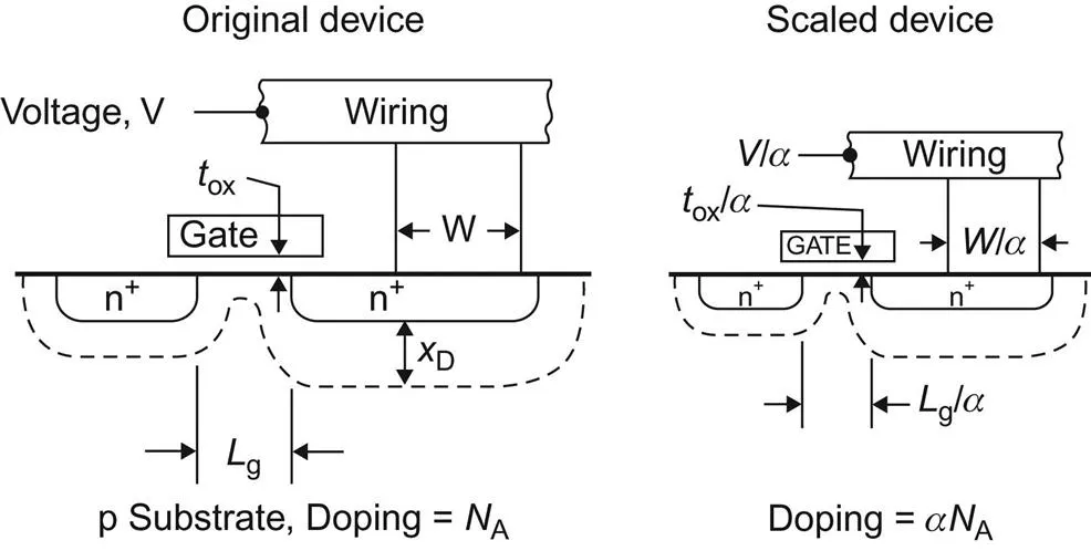
In order to keep the same electric field pattern as the original transistor in the substrate of the scaled device, original transistor impurity doping concentration is increased for the smaller device.
Taken along with the reduced applied voltage, this reduces the size of the depletion regions, identified by xd in Fig. 5.1, underneath all three transistor electrodes (gate, source, and drain) [3]. In general, these depletion regions...
Table of contents
- Cover image
- Title page
- Table of Contents
- Copyright
- Dedication
- List of Contributors
- Biographies
- Preface
- Section I: Scaling
- Section II: Thin Film Deposition Equipment & Processing
- Index
Frequently asked questions
Yes, you can cancel anytime from the Subscription tab in your account settings on the Perlego website. Your subscription will stay active until the end of your current billing period. Learn how to cancel your subscription
No, books cannot be downloaded as external files, such as PDFs, for use outside of Perlego. However, you can download books within the Perlego app for offline reading on mobile or tablet. Learn how to download books offline
We are an online textbook subscription service, where you can get access to an entire online library for less than the price of a single book per month. With over 1.5 million books across 990+ topics, we’ve got you covered! Learn about our mission
Look out for the read-aloud symbol on your next book to see if you can listen to it. The read-aloud tool reads text aloud for you, highlighting the text as it is being read. You can pause it, speed it up and slow it down. Learn more about Read Aloud
Yes! You can use the Perlego app on both iOS and Android devices to read anytime, anywhere — even offline. Perfect for commutes or when you’re on the go.
Please note we cannot support devices running on iOS 13 and Android 7 or earlier. Learn more about using the app
Please note we cannot support devices running on iOS 13 and Android 7 or earlier. Learn more about using the app
Yes, you can access Handbook of Thin Film Deposition by Krishna Seshan,Dominic Schepis in PDF and/or ePUB format, as well as other popular books in Technology & Engineering & Materials Science. We have over 1.5 million books available in our catalogue for you to explore.