- 334 pages
- English
- ePUB (mobile friendly)
- Available on iOS & Android
eBook - ePub
About this book
Nanostructured Thin Films: Fundamentals and Applications presents an overview of the synthesis and characterization of thin films and their nanocomposites. Both vapor phase and liquid phase approaches are discussed, along with the methods that are sufficiently attractive for large-scale production. Examples of applications in clean energy, sensors, biomedicine, anticorrosion and surface modification are also included. As the applications of thin films in nanomedicine, cell phones, solar cell-powered devices, and in the protection of structural materials continues to grow, this book presents an important research reference for anyone seeking an informed overview on their structure and applications.
- Shows how thin films are being used to create more efficient devices in the fields of medicine and energy harvesting
- Discusses how to alter the design of nanostructured thin films by vapor phase and liquid phase methods
- Explores how modifying the structure of thin films for specific applications enhances their performance
Trusted by 375,005 students
Access to over 1.5 million titles for a fair monthly price.
Study more efficiently using our study tools.
Information
Chapter 1
Nanostructured thin films–background, preparation and relation to the technological revolution of the 21st century
Maria Benelmekki a , b and Andreas Erbe b a College of Engineering, Swansea University Bay Campus, Swansea, United Kingdom b Department of Materials Science and Engineering, NTNU, Norwegian University of Science and Technology, Trondheim, Norway
Abstract
Thin film technology is a mature field encompassing a wide range of applications such as electronics, optical communications, and biosystems. The list of potential applications is practically endless with an impact in nearly every industrial sector. Many thin film applications are linked to developments in the semiconductor industry such as thin film transistors, large-area displays, microelectromechanical/nanoelectromechanical systems, planar waveguides, and magnetic data storage. This introductory chapter provides a new insight into nanostructured thin films. It gives an overview on the application on thin films, a general classification of nanostructured thin films, a brief introduction of the methods of synthesis of these nanostructures. Finally, the chapter discusses the challenges faced during the scale-up of the processes and the most important aspects to be considered when planning the industrialization of a developed process.
Keywords
2D materials; 2D nanocomposites; ALD self-assembly; CVD; Electrodeposition; Nanostructured thin films; PVD; Thin films
1. An overview of thin films and nanotechnology
Nowadays, the use of thin films to enhance the physical and chemical properties of materials is the most common practice in almost all the fields. Thin solid films have been used in many types of engineering systems and have been adapted to fulfill a wide variety of functions. For example, important and great developments in thin film technology were achieved allowing a rapid development of miniaturization of electronic devices [1,2]. In such devices, confinement of electric charge depends on the interfaces between materials with differing electronic properties. In addition, the need for thin materials of high quality, reproducibility, and reliability was the driving force for the rapid development and the significant progress of thin film growth techniques. More recently, progress in the physics of material structures that rely on quantum confinement of charge carriers continues to revolutionize the area and leads to new challenges for thin film synthesis, characterization, and modeling. Another example is the integration of thin films in microelectromechanical systems. A piezoelectric or piezoresistive thin film deposited on a silicon membrane can be used to detect electronically a membrane defect in response to a pressure applied on its surface. Devices based on thin film technology are used as microphones in hearing aids, monitors of blood pressure during exercise, electronically positioned thin film mirrors on flexible supports in optical display systems, and probes for detecting the degree of ripeness of fruits [2–4]. Another field of application is food packaging where multifunctional thin films are used as antibacterial and gas barriers [3–5].
Greene in his recent review [1] provided a concise overview on thin film history and applications. He discussed the implementation of thin films since ∼2500 BC, when gold films were used as decorative and later as optical coating (Fig. 1.1) [6]. The reader can refer to this review paper for a general overview on the evolution of thin film technology.
Fig. 1.2 illustrates three examples of the current thin film use in daily life: (A) copper metallization layers for electronic communication among billions of transistors in a silicon-integrated circuit; (B) coated glass in office buildings for which the thin films are designed to enhance energy efficiency and comfort by, depending on the time of year and latitude, reflecting ultraviolet and infrared sunlight, while transmitting visible light, to minimize air conditioning usage, or reflecting infrared radiation from within offices to minimize heating; and (C) coated cutting tools developed to reduce friction and wear during use and, hence, increase tool lifetime [1].
Other common examples include magnetic thin films for electronic data storage; transparent conductive oxide and absorber layers in solar cells; thin film resistors and dielectrics; catalytic layers for gas sensing; superconducting thin films for high-frequency devices, data storage, and magnetic circuitry; protective layers for automotive and airplane parts against corrosion, friction; and multiple layers on eyeglasses to correct vision, minimize ultraviolet light transmission, and provide scratch resistance [1,2,7].
For the last century, thin films have attracted the interest of scientists and engineers and have been a subject of intensive research and development. Within this period, the field of materials science and engineering has emerged as a key factor for important developments in all areas of engineering and applied science. The study of thin film materials has been one of the unifying themes in the development of the field during this period. The area encompasses films bonded to relatively thick substrates, multilayer materials, patterned films on substrates and free-standing films. The driving forces toward modern engineering process were the significant advances in the methods of synthesis, processing, and nanoscale characterization of these materials. At the beginning of the 21st century, the United States National Academy of Engineering [4] reported the outcome of a project intended to identify the 20 most significant engineering achievements of the preceding century. The study evidenced that thin film materials represent a major component of the advances and achievements in materials technology during the second half of the 20th century: electronics, computers, health technologies, laser and fiber optics, among others. The development and improvement of many methods and techniques for the growth and control of thin films, resulted in their widely use and exploitation in the industry. The early industrialization of thin film technology represented the key factor for further development and improvement of the deposition techniques.
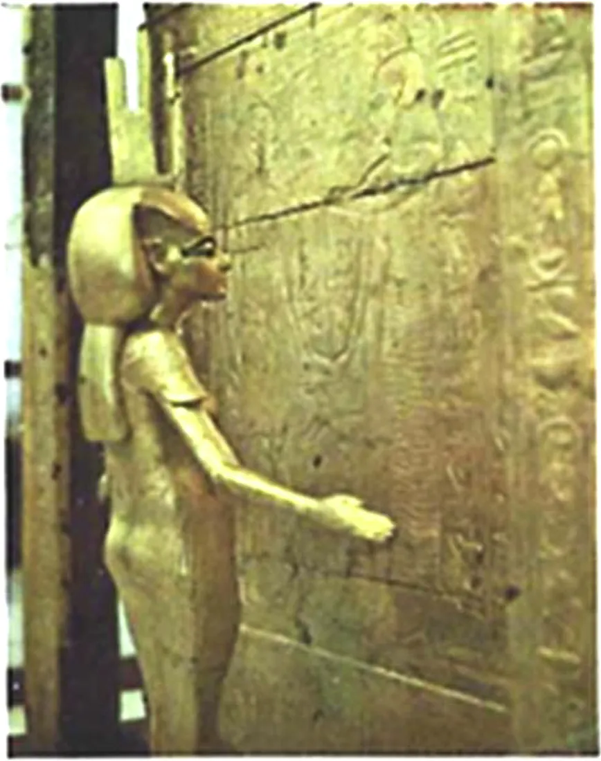
Reproduced from J.E. Greene, J. Vac. Sci. Technol. A, 35 (2017) 05C204; T.G.H. James, Gold Bull. 5 (1972) 38–42. Copyright 1972 by Peter Clayton under CC BY 4.0.

Reproduced from J.E. Greene, J. Vac. Sci. Technol. A 35 (2017) 05C204 under CC BY 4.0.
Organic thin films have long been used to tailor surface properties. In the modern natural sciences pioneered by Agnes Pockels [8], a Langmuir–Blodgett (LB) transfer of self-assembled films to solid substrat...
Table of contents
- Cover image
- Title page
- Table of Contents
- Frontiers of Nanoscience
- Copyright
- Contributors
- Chapter 1. Nanostructured thin films–background, preparation and relation to the technological revolution of the 21st century
- Chapter 2. Micro- and nanostructured piezoelectric polymers: Fundamentals and application
- Chapter 3. Nanostructured flexible PVDF and fluoropolymer-based hybrid films
- Chapter 4. Two-dimensional nanostructures for biomedical applications
- Chapter 5. Nanostructured magnetite thin films: An avenue for spintronics
- Chapter 6. Dynamic effects in siloxane PECVD coatings
- Chapter 7. Scanning thermal microscopy—a tool for thermal measurement in the nanoscale
- Chapter 8. Interface and surface properties of oxide–organic hybrid nanostructures: From charge transfer to degradation effects
- Chapter 9. Coatings and surfaces with hydrophobic and anti-icing properties
- Chapter 10. Spectroscopic and electrical properties of hybrid thin films for solar cell applications
- Chapter 11. Biomedical applications of ultrathin atomic layer deposited metal oxide films on polymeric materials
- Index
Frequently asked questions
Yes, you can cancel anytime from the Subscription tab in your account settings on the Perlego website. Your subscription will stay active until the end of your current billing period. Learn how to cancel your subscription
No, books cannot be downloaded as external files, such as PDFs, for use outside of Perlego. However, you can download books within the Perlego app for offline reading on mobile or tablet. Learn how to download books offline
Perlego offers two plans: Essential and Complete
- Essential is ideal for learners and professionals who enjoy exploring a wide range of subjects. Access the Essential Library with 800,000+ trusted titles and best-sellers across business, personal growth, and the humanities. Includes unlimited reading time and Standard Read Aloud voice.
- Complete: Perfect for advanced learners and researchers needing full, unrestricted access. Unlock 1.5M+ books across hundreds of subjects, including academic and specialized titles. The Complete Plan also includes advanced features like Premium Read Aloud and Research Assistant.
We are an online textbook subscription service, where you can get access to an entire online library for less than the price of a single book per month. With over 1.5 million books across 990+ topics, we’ve got you covered! Learn about our mission
Look out for the read-aloud symbol on your next book to see if you can listen to it. The read-aloud tool reads text aloud for you, highlighting the text as it is being read. You can pause it, speed it up and slow it down. Learn more about Read Aloud
Yes! You can use the Perlego app on both iOS and Android devices to read anytime, anywhere — even offline. Perfect for commutes or when you’re on the go.
Please note we cannot support devices running on iOS 13 and Android 7 or earlier. Learn more about using the app
Please note we cannot support devices running on iOS 13 and Android 7 or earlier. Learn more about using the app
Yes, you can access Nanostructured Thin Films by Maria Benelmekki,Andreas Erbe in PDF and/or ePUB format, as well as other popular books in Technology & Engineering & Materials Science. We have over 1.5 million books available in our catalogue for you to explore.