Nanostructured silicon-germanium (SiGe) opens up the prospects of novel and enhanced electronic device performance, especially for semiconductor devices. Silicon-germanium (SiGe) nanostructures reviews the materials science of nanostructures and their properties and applications in different electronic devices.The introductory part one covers the structural properties of SiGe nanostructures, with a further chapter discussing electronic band structures of SiGe alloys. Part two concentrates on the formation of SiGe nanostructures, with chapters on different methods of crystal growth such as molecular beam epitaxy and chemical vapour deposition. This part also includes chapters covering strain engineering and modelling. Part three covers the material properties of SiGe nanostructures, including chapters on such topics as strain-induced defects, transport properties and microcavities and quantum cascade laser structures. In Part four, devices utilising SiGe alloys are discussed. Chapters cover ultra large scale integrated applications, MOSFETs and the use of SiGe in different types of transistors and optical devices.With its distinguished editors and team of international contributors, Silicon-germanium (SiGe) nanostructures is a standard reference for researchers focusing on semiconductor devices and materials in industry and academia, particularly those interested in nanostructures.
- Reviews the materials science of nanostructures and their properties and applications in different electronic devices
- Assesses the structural properties of SiGe nanostructures, discussing electronic band structures of SiGe alloys
- Explores the formation of SiGe nanostructuresfeaturing different methods of crystal growth such as molecular beam epitaxy and chemical vapour deposition
Trusted by 375,005 students
Access to over 1.5 million titles for a fair monthly price.
Structural properties of silicon–germanium (SiGe) nanostructures
E. Kasper and H.-J. Herzog, University of Stuttgart, Germany
Abstract:
The heterostructure SiGe/Si has contributed to a large extent to an understanding of lattice mismatched heterostructures and this understanding has led to rapidly increasing exploitation of SiGe in modern microelectronics. In this chapter crystallographic data of silicon–germanium alloys such as crystal structure and lattice parameters and the phase diagram are reviewed. The basic concepts of equilibrium strain and strain relaxation by misfit dislocations are described in the section on critical thickness. The lattice mismatch either causes strain or results in generation of misfit dislocations at the interface. X-ray diffraction is unrivalled as a tool to analyze heteroepitaxial layers.
Key words:
heterostructure
silicon–germanium alloy
lattice structure
phase diagram
lattice mismatch
strain
misfit dislocations
critical thickness
X-ray diffraction
1.1 Introduction
A reliable set of structural data is essential for many investigations of both epilayers, and bulk material. Even the structural assessment and analysis of SiGe epilayers, which are presently of enormous interest for novel and high-performance device applications, require the knowledge of sufficiently precise material data. In this chapter some crystallographic data of silicon–germanium alloys, such as crystal structure and lattice parameters and the phase diagram, are reviewed. For a more complete collection of data the reader is referred to standard volumes on physical properties of semiconductors, e.g. the Landolt-Börnstein Series [1,2], or specific data reviews, e.g. the EMIs Datareview series [3,4].
The technically important structure SiGe/Si serves also as a model system for lattice mismatched heterostructures because chemical effects are less pronounced than in systems with elements from different columns of the periodic table. The basic concepts of equilibrium strain and strain relaxation by misfit dislocations are described in the section on critical thickness. The conceptual structure of this section follows that given in a lecture on ‘semiconductor Technology’ by one of the authors (Erich Kasper).
1.2 Crystal structure
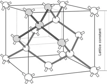
Silicon and germanium, which both crystallize in the diamond lattice, are completely miscible, forming Si1–xGex solid solutions with x ranging from 0 to 1. The space lattice of diamond consists of two face-centred-cubic (fcc) lattices which are displaced a quarter of the space diagonal. A perspective drawing of the unit cell is depicted in Fig. 1.1. The space group of the diamond structure is 0 h–Fd3m. The cubic unit cell contains eight atoms that occupy the following positions:
1.1 Diamond crystal structure. Each atom is tetrahedrally bonded to its four nearest neighbours as displayed by the rods.
The fractions denote the height above the base in units of the cube edge. In this structure each atom is bonded to four nearest neighbours with a distance of
arranged at the corners of a regular tetrahedron and to 12 next-nearest neighbours. Four tetrahedra form the non-primitive unit cell. The diamond structure is the result of the covalent bonding between the atoms represented by the rods in Fig. 1.1. The diamond lattice is not very compact. Only 34% of the available space is filled with hard spheres.
1.3 Lattice parameters
To date, the most precise and comprehensive determination of bulk lattice parameters (and densities) across the whole Si1–xGex system has been carried out by Dismukes et al. [5], including measurement of the variation of lattice parameters with temperature up to 800 °C for some alloys. In Table 1.1 the lattice parameters of Si1–xGex alloys at 25 °C are listed for composition intervals of 5 at% Ge. The data reveal a small deviation from Vegard’s law, which means that the SiGe alloy parameters are determined by a linear interpolation of the parameters of the end-point elements Si and Ge.
Table 1.1
Lattice parameter a of Si1–xGex alloys for x from 0 to 100 at% in 5% steps after [5]. The right column gives the deviation from Vegard’s law Δ
The depart...
Table of contents
Cover image
Title page
Table of Contents
Copyright
Contributor contact details
Preface
Part I: Introduction
Part II: Formation of nanostructures
Part III: Material properties of SiGe nanostructures
Part IV: Devices using silicon, germanium and silicon–germanium (Si, Ge and SiGe) alloys
Index
Frequently asked questions
Yes, you can cancel anytime from the Subscription tab in your account settings on the Perlego website. Your subscription will stay active until the end of your current billing period. Learn how to cancel your subscription
No, books cannot be downloaded as external files, such as PDFs, for use outside of Perlego. However, you can download books within the Perlego app for offline reading on mobile or tablet. Learn how to download books offline
Perlego offers two plans: Essential and Complete
Essential is ideal for learners and professionals who enjoy exploring a wide range of subjects. Access the Essential Library with 800,000+ trusted titles and best-sellers across business, personal growth, and the humanities. Includes unlimited reading time and Standard Read Aloud voice.
Complete: Perfect for advanced learners and researchers needing full, unrestricted access. Unlock 1.5M+ books across hundreds of subjects, including academic and specialized titles. The Complete Plan also includes advanced features like Premium Read Aloud and Research Assistant.
Both plans are available with monthly, semester, or annual billing cycles.
We are an online textbook subscription service, where you can get access to an entire online library for less than the price of a single book per month. With over 1.5 million books across 990+ topics, we’ve got you covered! Learn about our mission
Look out for the read-aloud symbol on your next book to see if you can listen to it. The read-aloud tool reads text aloud for you, highlighting the text as it is being read. You can pause it, speed it up and slow it down. Learn more about Read Aloud
Yes! You can use the Perlego app on both iOS and Android devices to read anytime, anywhere — even offline. Perfect for commutes or when you’re on the go. Please note we cannot support devices running on iOS 13 and Android 7 or earlier. Learn more about using the app
Yes, you can access Silicon-Germanium (SiGe) Nanostructures by Y. Shiraki,N Usami,Yasuhiro Shiraki,Noritaka Usami in PDF and/or ePUB format, as well as other popular books in Technology & Engineering & Condensed Matter. We have over 1.5 million books available in our catalogue for you to explore.