- 426 pages
- English
- ePUB (mobile friendly)
- Available on iOS & Android
eBook - ePub
Fundamentals and Applications of Nanophotonics
About this book
Fundamentals and Applications of Nanophotonics includes a comprehensive discussion of the field of nanophotonics, including key enabling technologies that have the potential to drive economic growth and impact numerous application domains such as ICT, the environment, healthcare, military, transport, manufacturing, and energy.
This book gives readers the theoretical underpinnings needed to understand the latest advances in the field. After an introduction to the area, chapters two and three cover the essential topics of electrodynamics, quantum mechanics, and computation as they relate to nanophotonics.
Subsequent chapters explore materials for nanophotonics, including nanoparticles, photonic crystals, nanosilicon, nanocarbon, III-V, and II-VI semiconductors. In addition, fabrication and characterization techniques are addressed, along with the importance of plasmonics, and the applications of nanophotonics in devices such as lasers, LEDs, and photodetectors.
- Covers electrodynamics, quantum mechanics and computation as these relate to nanophotonics
- Reviews materials, fabrication and characterization techniques for nanophotonics
- Describes applications of the technology such as lasers, LEDs and photodetectors
Trusted by 375,005 students
Access to over 1.5 million titles for a fair monthly price.
Study more efficiently using our study tools.
Information
1
Introduction to nanophotonics
J.W. Haus University of Dayton, Dayton, OH, USA
Abstract
This chapter serves as a brief introduction to nanophotonics and the topics are covered in greater detail and depth in the following chapters. The main themes of materials, fabrication, and characterization are discussed and connected to the development of photonic devices.
Keywords
Characterization; Chemical bonding; Fabrication; Materials; Top-down and bottom-up approachesIf I have seen further it is by standing on the shoulders of Giants.
Isaac Newton, from the Correspondence of Isaac Newton.
Nothing in life is to be feared, it is only to be understood. Now is the time to understand more, so that we may fear less.
Marie Skłodowska-Curie, quoted in Our Precarious Habitat (1973) by Melvin A. Benarde, p. v.
1.1. Introduction
We are embarking on a journey across the broad subject of nanophotonics. Nanophotonics activities engage researchers in many disciplines: optics; physics; chemistry; electrical, chemical, and mechanical engineering; materials science; biology; and mathematics. The range of activities is far too large to be captured by a single tome. Therefore, the number of topics covered in this book is narrowed by our personal choices. We divide the field of nanophotonics into three broad categories, which are distinguished by their functionality: materials, fabrication, and characterization. Of course, the prefix nano can be inserted in front of all three words for emphasis, but let us not overuse the term at the outset. The three aspects of nanophotonics are analogous to the legs of a three-legged stool with nanophotonics resting on top of them, as illustrated in Figure 1.1. Researchers and engineers apply all three of these areas to solve technological challenges. The image conveys our bias that removing one of the topics would leave out essential knowledge that we believe every student of nanophotonics should be familiar with.
The required breadth of the field is also conducive to the formation of collaborations within and across institutions; the members of the collaboration contribute their expertise in a specific field to the completion of the project. The student or new researcher in the field will find it advantageous to possess knowledge of the basic principles for all three aspects to effectively communicate with colleagues and to understand the main issues from different perspectives. A solid foundation in all three aspects provides access to a broader range of literature and gives deeper insights into physical limitations. This book was conceived to provide readers with a working knowledge of the principles in several fields.
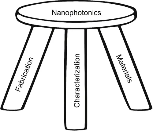
Figure 1.1 Three legs of a stool illustration to emphasize the three aspects of nanophotonics.
1.2. Materials
Technological progress is often based on the development of new materials. To highlight that point in a historical context, recall that two of the three named archaeological periods of man's ascent are named after materials technology—the bronze and iron ages. The further development of new materials has proceeded through the millennia and today, we are guided by a deeper quantitative understanding of materials' composition and properties.
Modern-age materials are much more sophisticated, but the main technology drivers are the same. In the modern era, silicon has emerged as one of the most important materials with applications ranging from electronics to micro-electro-mechanical systems (MEMS) to electronic sensors to photonics. There is market pressure to fabricate devices that have new functionality and can be produced using materials that are widely available and inexpensive. Silicon is one of the most abundant elements on Earth, second only to oxygen, making it an ideal material for many technological applications.
Today nanophotonics research is devoted to creating new materials with functionality that is not ordinarily available by processing natural elements, alloys, or compounds. The elements of the periodic table are cast into a form that is not normally found in nature. The purpose is to elicit a new response to electronic current or optical waves. The new response may be potentially useful for fabricating new devices or for making a new instrument with improved resolution.
The abundance of the elements is another important consideration in pursuing new technologies. Figure 1.2 is a plot of the elements' relative abundance found in the earth. The high abundance of elements such as hydrogen, silicon, oxygen, iron, carbon, and nitrogen (abundant in the atmosphere) make them inexpensive and easy to procure. Other in-demand elements may have a supply that is controlled by a single country; thus, they are subject to political crises or pressures. For instance, the rare-earth metals have found important uses in electronics, lighting, displays, and communications technologies. Fortunately, the amount of rare-earth elements used in many of these applications is tiny, and global-scale use is not affected by their market availability. In developing new materials with desired functionality, one may be driven by the need to reduce or eliminate expensive or geopolitical elements. A commercial product that uses scarce, expensive, or geographically concentrated elements will not be sustainable on a massive scale over a long period of time.
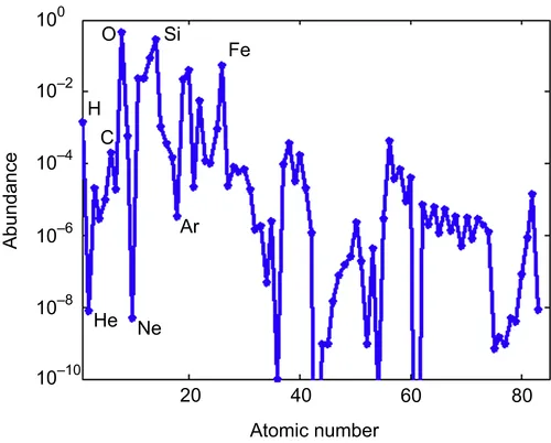
Figure 1.2 Abundance (by mass) of the elements in the Earth's upper continental crust up to element 82. Plotted from data available from http://en.wikipedia.org/wiki/Abundance_of_the_chemical_elements.
Chemical and physical properties of materials are deeply connected to the quantum mechanics of the hydrogen atom. The framework for understanding atomic spectra is based on the Bohr model of electrons in orbits around a small, positively charged nucleus. His quantization of the angular momentum of the electrons prevented them from collapsing to the nucleus, as would be expected from classical Newtonian dynamics. The essence of the Bohr model was captured in quantum mechanics, which describes electrons in their orbital states. For the quantum solution of the hydrogen atom, the Coulomb attraction of the electron to the proton yields a set of states that are labeled by a set of quantum numbers describing the energy, angular momentum, and the spin momentum of the electrons. Surprisingly, the simple model of the hydrogen atom extends to the electronic states of multielectron atoms; the occupation of electronic states conforms to state designations that are identical to the hydrogen atom.
The treatment of molecules and solids is organized around the atomic orbital states of constituent atoms. However, to understand the electron bonding energies and geometry, such as bond angles and lattice symmetry, multiple electronic states are combined. The bonding length and direction between atoms, although closely connected to the atomic states, are based on simple electronic principles; namely, paired electrons with opposite intrinsic spin are shared between atoms to form a covalent bond. The covalent bond angles are based on electron pairs shared between atoms and can be understood by using a linear combination of atomic orbitals (LCAOs). In chemistry, the LCAO is termed hybridization and is discussed in Chapter 4. The LCAO is a simplification that uses valence electron wave functions as a set of basis states to calculate a wide range of physical properties. The technique provides a simple physical description of the bond angles in molecular and lattice systems.
Electron interactions manifest different bonding mechanisms that may be identified from their electronic density distributions. Metallic bonding has electron density delocalized throughout the solid, whereas covalent bonds have valence electron density largely localized between the atomic nearest-neighbor pairs. The malleability of many metals is an indication that the metallic bonds are relatively weak. Similar to covalent bonding, ionic bonding is based on electron density displacement between the pair of atoms to form a cohesive crystal; the atoms called cations give up the electrons, leaving a net-positive charge and the electron has a density displaced more to the other atoms called anions. Ionic and covalent bonds can both be present to some degree in solids. The covalent bonds are highly dependent on orientation because of the bonding orbitals, whereas the ionic bonds depend on the difference in affinity of the atoms to attract an electron, so-called electronegativity. Finally, there is a fourth type of bonding that is commonly mentioned called van der Waals bonds, which is dominant for atoms with closed electron shells (e.g., inert gas atoms). The electrons in inert gas atoms are tightly bound to the nuclei and they are not shared with neighboring atoms. For inert atoms, their bonding in the solid state is promoted by induced atomic dipoles on the atoms due to quantum fluctuations, which are van der Waals interactions. This form of bonding is weak.
Scientists and researchers refuse to be confined by the materials refined from naturally occurring compounds. Chemists and materials scientists have tweaked the growth and synthesis processes to create new materials or nanostructured materials that exhibit unusual electronic and optical properties. For instance, there has been enormous progress made in designing and fabricating quantum-confined structures that are now commercially available in semiconductor lasers and photodetectors. Recent activities have led to the development of novel, fabricated materials' classifications—called photonic crystals, plasmonics, and metamaterials—that are designed to accentuate specific properties of light. These specific materials are introduced and discussed in subsequent chapters of this book. Because each class of new materials have exposed the community to novel physical concepts, they have spawned worldwide research efforts to discover new applications for the novel laboratory materials. For instance, metals, also called plasmonic materials, have taken center stage with traditional applications in biosensing and potential applications in energy harvesting and photonic surfaces.
1.3. Fabrication and characterization
The techniques to create new photonic devices and optical materials have been divided into two areas—top-down and bottom-up approaches—and their general features are illustrated in Figure 1.3. The top-down approach is exemplified by the fabrication techniques used to make electronic circuitry and MEMS devices, which have become ubiquitous elements in commercial devices from phones and iPads to automobiles. The starting point is a wafer substrate material that is a building block with required characteristics. The wafer has material removed, added, or doped using the available suite of...
Table of contents
- Cover image
- Title page
- Table of Contents
- Related titles
- Copyright
- List of contributors
- Woodhead Publishing Series in Electronic and Optical Materials
- Preface
- 1. Introduction to nanophotonics
- 2. Electrodynamics for nanophotonics
- 3. Quantum mechanics and computation in nanophotonics
- 4. Materials
- 5. Nanofabrication
- 6. Nanocharacterization
- 7. Effective medium theories
- 8. Plasmonics
- 9. Metamaterials
- 10. A dynamical, classical oscillator model for linear and nonlinear optics
- 11. Nanophotonic devices
- Index
Frequently asked questions
Yes, you can cancel anytime from the Subscription tab in your account settings on the Perlego website. Your subscription will stay active until the end of your current billing period. Learn how to cancel your subscription
No, books cannot be downloaded as external files, such as PDFs, for use outside of Perlego. However, you can download books within the Perlego app for offline reading on mobile or tablet. Learn how to download books offline
Perlego offers two plans: Essential and Complete
- Essential is ideal for learners and professionals who enjoy exploring a wide range of subjects. Access the Essential Library with 800,000+ trusted titles and best-sellers across business, personal growth, and the humanities. Includes unlimited reading time and Standard Read Aloud voice.
- Complete: Perfect for advanced learners and researchers needing full, unrestricted access. Unlock 1.5M+ books across hundreds of subjects, including academic and specialized titles. The Complete Plan also includes advanced features like Premium Read Aloud and Research Assistant.
We are an online textbook subscription service, where you can get access to an entire online library for less than the price of a single book per month. With over 1.5 million books across 990+ topics, we’ve got you covered! Learn about our mission
Look out for the read-aloud symbol on your next book to see if you can listen to it. The read-aloud tool reads text aloud for you, highlighting the text as it is being read. You can pause it, speed it up and slow it down. Learn more about Read Aloud
Yes! You can use the Perlego app on both iOS and Android devices to read anytime, anywhere — even offline. Perfect for commutes or when you’re on the go.
Please note we cannot support devices running on iOS 13 and Android 7 or earlier. Learn more about using the app
Please note we cannot support devices running on iOS 13 and Android 7 or earlier. Learn more about using the app
Yes, you can access Fundamentals and Applications of Nanophotonics by Joseph W. Haus in PDF and/or ePUB format, as well as other popular books in Technology & Engineering & Optics & Light. We have over 1.5 million books available in our catalogue for you to explore.